75th Anniversary of the Transistor
History and Emerging Designs of Power Transistors

Electricity was playing a major role in the lives of people by the middle of the 20th century. Electric lighting, pioneered by Edison, had improved productivity, quality of life, and safety by illumination of our streets, factories, and residences. Refrigeration, enabled by efficient motors, had transformed the storage of perishable foods in homes while preserving them during delivery from farms to the market. The replacement of mechanical actuators for these application with electronic switches became a possibility after the invention of the bipolar transistor (Shockley, Bardeen, and Brattain, Bell Labs, 1947). For applications operating at high power levels, the ideal electronic switches must exhibit the following characteristics: (a) high voltage blocking capability; (b) low on-state voltage drop to reduce conduction losses; (c) fast switching capability for the voltage and current to minimize switching losses; (d) ability to tolerate simultaneous imposition of high voltage and current during the switching transient for ruggedness; (e) control of current using a small voltage with low drive currents to allow integration of the drive electronics; and (f) current saturation under drive voltage control to avoid the need for snubber elements. In addition, an ideal power transistor should be able operate symmetrically in the first and third quadrants. The quest to create a power transistor that satisfies these requirements has driven innovations in the technology during the last 60 years.
This article highlights important power transistor innovations that have occurred since the 1960s allowing displacement of analog power control (phase control) with digital power control (pulse width modulation). These innovations initially required changes in device architecture and physics for silicon based transistors. Subsequently, even greater performance enhancements were achieved by replacing silicon with wide band gap semiconductor materials.
The power bipolar transistor architecture (Fig. 1 left) was a departure from the signal transistor due to the need for supporting the high voltages and controlling the high currents required in power applications. The power transistor requires a vertical structure with one of the high current terminals (collector) located at the bottom of the chip, with the other high current terminal (emitter) formed at the top. The base terminal must be interdigitated with the emitter because on-state current flow concentrates at the emitter edges due to the emitter crowding effect. A thick drift region with low doping concentration is required to support the high voltages, resulting in a large on-state resistance despite some conductivity modulation. Most significantly, a large base width is necessary to avoid reach-through limited breakdown, resulting in a low current gain (typically < 10 in the on-state). A large reverse base drive current is needed during turn-off to shorten the storage time, resulting in a current gain of only 2. Bulky and complex base drive circuits were consequently needed, which created reliability issues. The safe operating area of the power bipolar transistor was also poor, making addition of snubber components necessary.
The Darlington power bipolar transistor (Fig. 1 right) was developed to ameliorate the problem with low on-state current gain. It utilizes a base drive transistor T1 to provide drive current to the output transistor T2, as shown by its equivalent circuit in Fig. 1. This approach allowed increasing the current gain in the on-state but the turn-off gain was still poor. More significantly, the Darlington power transistor has a diode-like on-state characteristics because of current flow of transistor T1 through the base-emitter junction of transistor T2. This makes its on-state voltage drop much larger than the single bipolar transistor.

Figure 1. Evolution of Power Bipolar Transistors.
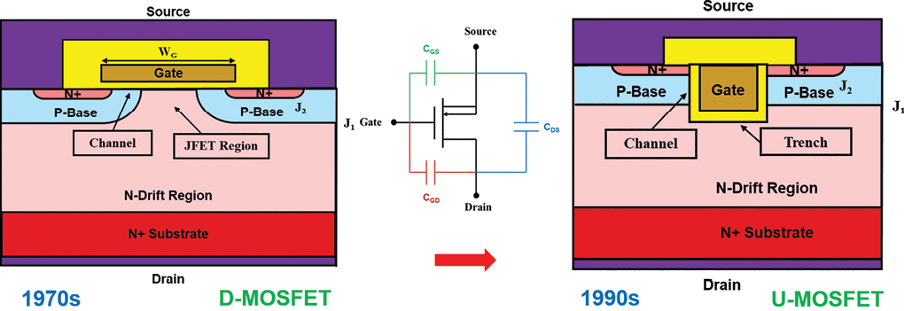
Figure 2. Evolution of Power Metal-Oxide-Semiconductor Field Effect Transistors.
The availability of the CMOS technology for integrated circuits enabled making power Metal-Oxide-Semiconductor Field Effect Transistors (MOSFETs) in the 1970s. The double-diffused or D-MOSFET (Fig. 2 left) was first commercialized by several companies (International Rectifier, Siliconix). It’s channel length is determined by the difference in diffusion depths of the P-base and N+ source regions, allowing short channel length (1 to 1.5 μm) to be achieved with 5 μm lithography process tolerances at that time. This device also has a vertical structure that contains a thick drift region with low doping concentration to support high voltages. It adds substantial on-state resistance for devices with high blocking voltages. On-state current flow occurs when a positive gate drive voltage is applied to the gate to induce an inversion layer at the surface of the P-base region to create a channel. The resistances of the channel and JFET regions contribute substantially to the total on-resistance for devices with low blocking voltages (< 100 V). This device exhibited most of the desired characteristics for the ideal electronic switch when the blocking voltage was less than 100 V.
The quest to realize lower on-resistance lead to the introduction of the power U-MOSFET (Fig. 2 right) by the industry in the 1990s (Siliconix). The JFET region resistance was eliminated using this structure allowing increasing the channel density as well. The U-MOSFETs reduced the on-resistance by a factor 3x for devices with 30 V ratings. However, the input capacitance for the devices (CGS in the equivalent circuit in Fig. 2) increased substantially slowing down the switching speed. However, the overall performance improvement made this structural design dominant in the 1990s.
A major breakthrough in enhancing the performance of silicon power MOSFETs occurred with the introduction of the two-dimensional charge-coupling concept in the 1990s. The first approach (Baliga, NCSU, U.S. Patent 5,637,898, 1997) was proposed with a source electrode inside a deep trench to produce the desired 2D charge-coupling. The GD-MOSFET (Fig. 3 left) with a linearly graded doping profile in the drift region was shown to greatly improve the electric field distribution in the drift region, allowing increasing its doping concentration far above (> 10x) that possible with the previous designs shown in Fig. 2. This approach reduced the drift region resistance well below what was previously considered the limit for ideal on-resistance for silicon material. The device structure, now commonly called the split-gate MOSFET (a misnomer because it contains only one gate electrode), has become the most popular product manufactured by leading power device companies (Alpha and Omega, Infineon) with blocking voltages up to 150 V. These devices are widely used for building power supplies to serve microprocessors and graphics chips in desktop and laptop computers.
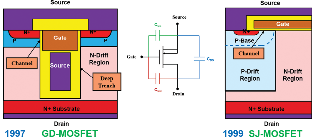
Figure 3. Evolution of Power Metal-Oxide-Semiconductor Field Effect Transistors.
The second approach (Lorenz, Infineon, ISPSD 1999) utilized a vertical junction produced by the addition of a deep P-type drift region operating in parallel with the N-type drift region to achieve the 2D charge-coupling. This device design (Fig. 3 right), commonly referred to as the super-junction (SJ) MOSFET, has become popular for making products with blocking voltages of 600 – 900 V. These devices are used in motor drive applications when switching losses are dominant. Products are available from many companies. (Infineon, ST Microelectronics).
The Insulated Gate Bipolar Transistor (IGBT) was invented, developed and commercialized in the early 1980s to replace the bipolar junction transistor due to its many short-comings (Baliga, General Electric, U.S. Patent 4,969,028, Filed 1980, Issued 1990). The device structure (Fig. 4 left) can be designed to be capable of blocking voltage in the first and third quadrant (Symmetric IGBT) at junctions J1 and J2 or only in the first quadrant (Asymmetric IGBT). The IGBT operates by creating an MOS-channel using a positive gate bias, which delivers the base drive current to the internal wide-base P-N-P bipolar transistor. Collector current flow is generated using both electrons via the channel and holes via the P-N-P transistor within the same drift region, called MOS-bipolar current transport. The device can be turned-off by reducing the gate voltage to zero to shut off the electron supply. The holes in the drift region are removed by recombination, creating a current tail that produces switching losses.
The proposed IGBT design was a radical departure because of employing a wide-base P-N-P transistor rather than the narrow-base N-P-N transistors used for power transistors at that time. Skeptics believed that this would severely limit the current flow making the device inferior to power bipolar transistors. My analysis, based upon high level injection physics within the N-base region (N-drift region), predicted P-i-N rectifier like on-state characteristics with low on-state voltage drop even at high current densities. This analysis was fortunately proven to be correct when actual devices were fabricated and tested.
A major hurdle for the IGBT was potential latch-up of the internal 4-layer thyristor, which could result in destructive failure. This issue was overcome using the deep P+ region (Fig. 4 left) added to the basic double-diffused MOSFET process (Baliga and Adler, General Electric, U.S. Patent 4,443,931, 1984). The IGBT was then believed to be limited to low operating frequencies, thus constraining its applications, because methods to control the minority carrier lifetime at that time led to damaging the MOS gate structure. Fortunately, I discovered a process that allowed using high energy electron irradiation to reduce the lifetime in the drift region followed by a low temperature annealing process that removed the damage in the gate oxide. This was crucial to creating IGBTs that could operate over a large range of switching speeds (Baliga, IEEE EDL, 1983), opening up a wide spectrum of applications within GE at first and then beyond.

Figure 4. Evolution of Insulated Gate Bipolar Transistors (IGBTs).
Based on my pitch in November 1980 projecting wide-spread impact of the IGBT within the Motor Drives, Lighting, Appliances, and Medical divisions at the General Electric Company, the Chairman, Jack Welch, approved full support for my development and commercialization of the IGBT. Based on this support, I was able to engineer and build the IGBT directly in the power MOSFET manufacturing line in less than 10 months. This had to be accomplished with no flaws during chip design and process definition, to ensure first pass success, due to the intense corporate scrutiny. This was a critical step in making the IGBT available in large quantities for use at GE to build the first adjustable speed motor drives for heat pumps, and novel lamps that were precursors of the compact fluorescent lamps that became commercially viable in the 1990s. Jack Welch embargoed any publication of information regarding the IGBT due its value to GE applications. This embargo was eventually broken by announcement of an IGBT product D94F4 by the Semiconductor Products Division in June 1983. It’s applications were promoted by GE (Baliga and Smith, IEEE APEC, 1983), which resulted in a “Product of the Year” Award. After the release of my publications by GE on the attributes of the IGBT from 1983 to 1985, products were developed and introduced by many companies (Toshiba, Mitsubishi Electric, Fuji Electric) in Japan starting in 1985.
IGBT innovations were also made in Europe (ABB, Siemens) in the 1990s with the transparent emitter design (Fig. 5 left). The P+ emitter region was replaced with a thin P-diffusion on the bottom of the wafer with low doping concentration to reduce the injection efficiency. This was found to reduce switching losses for very high voltage (> 4 kV) devices required to replace gate-turn-off (GTO) thyristors used for electric locomotive drives. This technology was rapidly optimized in Europe and Japan for wide spread use in urban and long distance public transportation.
An improvement to the trade-off between the on-state voltage drop and switching speed for the IGBT was achieved by employment of the trench-gate structure (Chang and Baliga IEEE IEDM, 1987). The trench-gate design (Fig. 4 right) increases channel density, providing more drive current to the internal bipolar transistor, to reduce on-state voltage drop. Another IGBT design innovation that was shown to improve the performance of high voltage IGBT devices was the deep trench structure (Toshiba, IEEE ISPSD, 1998) with a narrow P-base region (Fig. 5). This approach enhanced the conductivity modulation of the drift region resulting in lower on-state voltage drop.
Over the last 4 decades, the IGBT has become very popular for a large variety of applications (Baliga, The IGBT Device, Elsevier, 2015). It is used in all sectors (transportation, lighting, consumer, industrial, medical, etc.) of the economy to enhance the quality of life for billions of people around the world. The creation of the electronic ignition system using IGBTs for gasoline powered cars and trucks has reduced gasoline consumption by 1.8 trillion gallons from 1990-2020. The development of adjustable speed motor drives using IGBTs has reduced electricity consumption by 73,000 Tera-Watt-Hours from 1990–2020. The deployment of 20 billion compact fluorescent lamps using IGBT electronic ballasts has reduced electricity consumption by 59,900 Tera-Watt-Hours from 1990–2020. These applications of the IGBT have saved consumers $ 33.6 Trillion while reducing carbon-dioxide emissions by 181 Trillion pounds from 1990–2020 to mitigate global warming.
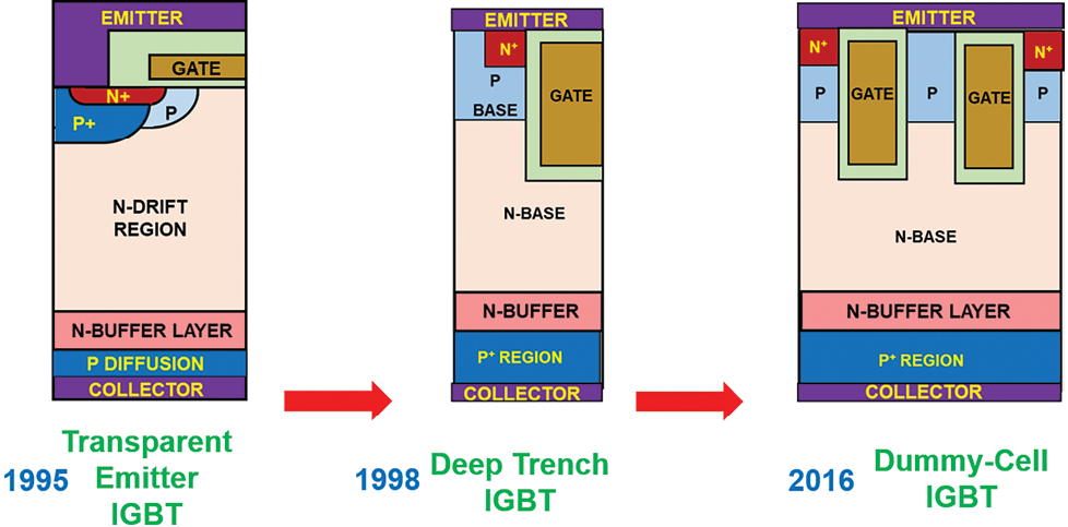
Figure 5. Evolution of Insulated Gate Bipolar Transistors (IGBTs).
All solar and wind power generation relies upon using the IGBT to convert the energy into a stable 50 or 60 Hz AC power that can be delivered to the grid. In addition, the IGBT is used for the inverters for driving the motors in electric cars manufactured by all automobile companies. It will therefore play an essential role in the elimination of fossil fuels in the electricity generation and transportation sectors to combat climate change.
The history of evolution of power devices includes a quantum leap in performance that was enabled by wide band gap semiconductor materials. The impact of replacing silicon with wide band gap semiconductors was first recognized by the derivation of an equation relating the drift region resistance in a vertical unipolar power device to the basic material properties, now commonly called Baliga’s Figure-of-Merit or BFOM (Baliga, GE, JAP, 1983; IEEE EDL, 1989). This equation predicted 13.7-fold reduction in resistance by using gallium arsenide and more than 100-fold reduction in resistance by using silicon carbide (SiC). The theory was validated in the 1990s, after the availability of 6H-SiC wafers, by fabricating 400 V Schottky rectifiers (Bhatnagar, McLarty and Baliga, IEEE EDL, 1992) and subsequently the first high performance SiC power MOSFETs. (Shenoy and Baliga, IEEE EDL, 1997). This required altering the power MOSFET structure to (a) shield the P-base region to prevent reach-through breakdown; (b) shield the gate oxide from high electric fields; and (c) employing accumulation channels to increase the channel mobility. The 4H-SiC planar-gate MOSFET structures that are now commercially available employ the shielded structures (Baliga, NCSU, U.S. Patent 5,543,637, 1996) with accumulation or inversion channels (Fig. 6).
The D-MOSFET process used for silicon power MOSFETs cannot be used for SiC devices due to insignificant diffusion of dopants in this material even at very high temperatures that lead to sublimation. The channel is therefore formed by staggered ion-implantation of the P and N-type dopants used to form the P-base and N+ source regions (Bhatnagar and Baliga, U.S. Patent 5,322,802, 1994; Shenoy, Cooper and Melloch, IEEE EDL, 1997). This requires high resolution photolithography to create the sub-micron channel lengths needed to achieve a low on-state resistance in the power MOSFETs. Commercial SiC planar-gate power MOSFETs are manufactured using this technology.
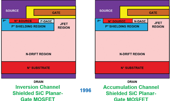
Figure 6. Evolution of Planar-Gate Silicon Carbide Power MOSFETs.
The reduction in switching power losses in motor drives by replacement of silicon IGBTs with SiC power MOSFETs was projected (Baliga, NCSU, Proceedings IEEE, 1994) and subsequently experimentally demonstrated (Fabre, et al., ALSTHOM, IEEE TPE, 2015). However, the cost of SiC power MOSFETs is at present more than 3-times that for the equivalent rated silicon IGBT, impeding its commercial viability. The strategy undertaken by the industry to overcome the higher cost of this technology is to operate the power electronics at a much higher frequency to reduce the cost of passive elements, such as inductors and filters, to offset the semiconductor cost. The operation of SiC power MOSFETs at higher frequencies requires design innovations to reduce drain current and voltage transient times during switching. Faster drain voltage transient times during switching can be achieved in SiC power MOSFETs by reducing the gate-drain charge.
One innovative design (Fig. 7 left) to achieve this employs a central-implanted P+ region inside the JFET region (Zhang, et al., CREE, IEEE ISPSD, 2015). Additional process steps are required to add the P+ region and it must be connected to the source electrode orthogonal to the cross-section. The second innovative approach (Fig. 7 middle) is the split-gate device design (Han, Baliga, and Sung, NCSU, IEEE EDL, 2017) where the width of the gate electrode is shortened over the JFET region. This design reduces the gate-drain charge by a factor of 2.4-times without any additional process steps. The third innovative design approach (Fig. 7 right) is the buffered-gate design (Han, Baliga, and Sung, NCSU, IEEE EDL, 2018) where the edge of the P+ shielding region is extended beyond the edge of the split-gate electrode. This design reduces the gate-drain charge by a factor of 6-times but requires an additional process step to include a second JFET region.
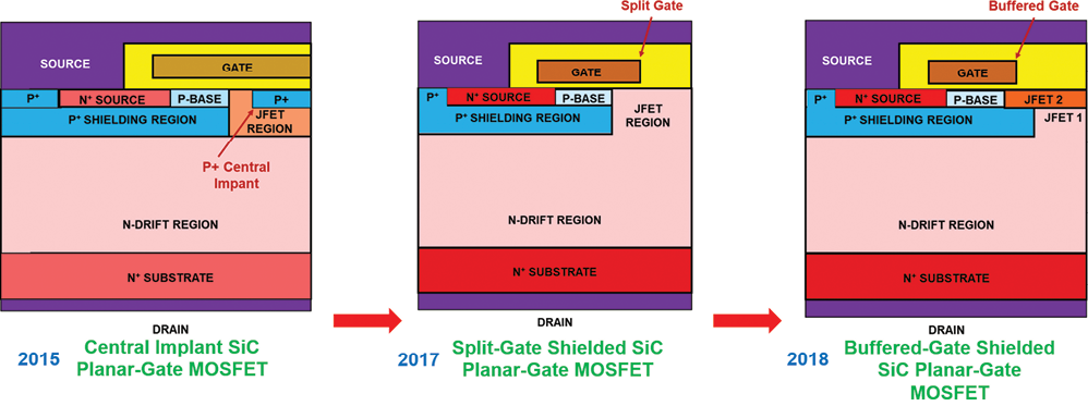
Figure 7. Evolution of Planar-Gate Silicon Carbide Power MOSFETs.
In typical voltage source inverters using the H-bridge topology with silicon IGBTs, it is necessary to connect an anti-parallel diode for operation of the adjustable speed drive for motors. In principle, the anti-parallel diode is not required for the SiC power MOSFET due to current flow via the P-N body diode. However, this approach has been found to result in high switching power losses due to the bipolar diode reverse recovery phenomenon at elevated temperatures. In addition, a phenomenon called bipolar degradation of the SiC power MOSFET was discovered where defects are generated in the drift region due to the P-N diode bipolar current flow. A discrete junction barrier controlled Schottky (JBS) diode (Baliga, GE, IEEE EDL, 1984; Held, Kaminski, and Niemann, ABB, Material Science Forum, 1998) can be connected across the SiC power MOSFET to prevent current flow via the body diode. This adds another packaged component with significant SiC chip area and cost. An innovative design (Fig. 8) integrates the JBS diode into the SiC power MOSFET cell structure (Sung and Baliga, NCSU, IEEE EDL, 2016). This structure was created by engineering the source contact process to simultaneously make a Schottky barrier contact to the drift region at the JBS diode and ohmic contacts to the N+ source and P+ shielding regions.

Figure 8. Evolution of Silicon Carbide Power MOSFETs.
As in the case of silicon power MOSFETs, trench-gate technology can be employed for SiC power MOSFETs to reduce the on-state resistance due to elimination of the JFET region and increase in channel density. The major challenge for this approach is a very high electric field in the gate oxide at the bottom of the trench that can lead to unreliable operation and even catastrophic failure. The first innovative design (Fig. 9 left) to solve this problem utilizes a P+ shielding region at the bottom of the trench which is connected to the source electrode orthogonal to the cross-section (Baliga, NCSU, U.S. Patent 5,396,085, 1995; Li, Cooper and Capano, Purdue University, IEEE EDL, 2002). The second approach (Fig. 9 middle) makes use of two trench regions (Harada, et al, Rohm, IEEE ISPSD, 2012), one to form the gate structure and a second deeper one for shielding the gate oxide. The third approach (Fig. 9 right) makes use of a shallow trench to form the gate structure and two deeper trenches to shield the gate oxide (Peters, et al, Infineon, PCIM 2017). In all three designs, a JFET region is created when shielding the gate oxide, which must be adequately doped to reduce the on-state resistance without degrading the breakdown voltage. Good on-state resistance, breakdown voltage and gate oxide shielding was observed with the first approach, while the lowest gate oxide electric field was observed for the third approach with a higher on-state resistance (Agarwal, Han and Baliga, NCSU, IEEE WiPDA, 2018).
As mentioned in the beginning of this article, the ‘holy grail’ for the power semiconductor community during the last 60 years has been to create a power switch with symmetric behavior in the first and third quadrants, gate voltage controlled output characteristics with current saturation, low on-state voltage drop, and fast switching capability. Power electronics engineers have used multiple discrete devices to assemble such a switch for use in matrix converters (Baliga and Han, NCSU, GOMACTech, 2018). A compact, monolithic 4-terminal bi-directional power switch, named the BiDFET, has been recently achieved (Baliga, NCSU, U.S. Patent 10,804,393, 2020; Han, et al., NCSU, IEEE ISPSD, 2020) by integration of two JBSFETs (Fig. 10). These devices will enable a new generation of power electronics that is more compact and efficient.

Figure 9. Evolution of Trench-Gate Silicon Carbide Power MOSFETs.

Figure 10. Monolithic SiC Bi-Directional Field Effect Transistor (BiDFET).
Excellent power devices can also be created using another wide bad gap semiconductor, gallium nitride (GaN). The ability to grow device quality epitaxial layers of GaN on low cost, large diameter, silicon substrates is a unique attribute of this approach. However, this requires fabrication of lateral high voltage power devices with inter-digitation of the drain, gate, and source electrodes, which can make the chip design challenging due to current crowding and parasitic metal resistances. The formation of a two-dimensional electron gas (commonly referred to as a 2D-gas) at the interface between GaN and aluminum gallium nitride (AlGaN) creates a layer with low sheet resistance to reduce on-state resistance. The first devices (Fig. 11 left) used a metal-gate (Schottky barrier) contact that produced normally-on behavior in the high-electron-mobility-transistor (HEMT) device. Since this is unacceptable for use in power circuits, this design was combined with a low-voltage silicon MOSFET to form the Baliga-Pair or Cascode topology (Baliga, NCSU, U.S. Patent 5,396,085, 1995; Transphorm and IRF products). Subsequently, normally-off GaN HEMT devices (Fig. 11 middle and right) were created using the recessed gate design (Saito, et al., IEEE TED, 2006) and P-GaN gate region (Holt, et al., IEEE IPES, 2010). The lateral configuration of these devices allows making multiple power transistors on the same chip to build compact power integrated circuits for applications such as laptop and cellphone chargers. The devices may be suitable for motor drives for electric vehicles but face a strong completion from the previously discussed SiC power MOSFET in this application space.

Figure 11. Gallium Nitride Lateral HEMT Power Devices.
Despite 40 years of progress, innovations in power semiconductor devices continue to enhance their performance. They have become essential technology for providing consumers with enhanced comfort, mobility, and quality of life. The transition from fossil fuels to renewable energy for our electricity needs and electric vehicles for our transportation can only be accomplished by utilizing power semiconductor devices.
Acronyms
APEC: Applied power Electronics Conference
EDL: Electron Device Letters
IEDM: International Electron Devices Meeting
IPES: International Conference on Integrated Power Electronic Systems
ISPSD: International Symposium on Power Semiconductor Devices and ICs
JAP: Journal of Applied Physics
PCIM: Power Conversion and Intelligent Motion Conference
TED: Transactions on Electron Devices
TPE: Transactions on Power Electronics
WiPDA: Wide bandgap semiconductor Power Device and Applications Workshop
Biography
_C.png)
Prof. Baliga is an internationally recognized expert on power semiconductor devices. He is a Member of the National Academy of Engineering and a Life Fellow of the IEEE. He spent 15 years at the General Electric Research and Development Center, Schenectady, NY, leading their power device effort and was bestowed the highest scientific rank of Coolidge Fellow. He joined NC State in 1988 as a Full Professor and was promoted to the rank of ‘Distinguished University Professor’ in 1997. Among his many NCSU honors, he was the recepient of the 1998 O. Max Gardner Award given by the North Carolina University Board of Governors to the one person within the 16 constituent universities who has made ‘the greatest contribution to the welfare of the human race’; and the 2011 Alexander Quarles Holladay Medal of Excellence, the highest honor at NCSU from the Board of Trustees. Prof. Baliga has authored/edited 22 books and over 700 scientific articles. He has been granted 122 U.S. Patents. The IEEE has recognized him numerous times—most recently with the highest award, the IEEE Medal of Honor. Scientific American magazine included him among the ‘Eight Heroes of the Semiconductor Revolution’ when commemorating the 50th anniversary of the invention of the transistor. Prof. Baliga invented, developed and commercialized the Insulated Gate Bipolar Trannsistor (IGBT) at GE. He was inducted into the National Inventors Hall of Fame as the sole inventor of the IGBT. The IGBT is extensively used in the consumer, industrial, lighting, transportation, medical, renewable energy, and other sectors of the economy. It has enabled enormous reduction of gasoline and electrical energy use, resulting in huge cost savings to consumers, and reduction of world-wide carbon dioxide emissions. A detailed description on the applications and social impact of the IGBT is available in one of his books. He received the National Medal of Technology and Innovation, the highest form of recognition given to an engineer by the United States Government, from President Obama in October 2011, at the White House; and the North Carolina Award for Science from Governor Purdue in October 2012, and the Global Energy Prize in 2015.
Transistors at 75—Past, Present, and Future
Early Transistors: Three Bell Labs researchers born on three continents invented the transistor 75 years ago—John Bardeen in America (Madison USA), William Shockley in Europe (Liverpool England), and Walter Brattain in Asia (Xiamen China). Another engineer, John Pierce, suggested the name “transistor” because it connects the new device to the already familiar terms: transconductance, resistor, etc.
Transistor became a household word when SONY introduced a shirt-pocket-size transistor radio using Texas Instruments transistors and a standard 9V battery in 1957 and went on to sell 6 million units of that model. IBM introduced the first mass-produced transistor computer in 1958.
From Ge to Si to Heterogeneous Integration: The early transistors were made with germanium. Around 1960, silicon became the preferred semiconductor because its larger bandgap greatly reduces the transistor leakage current especially when the transistors are hot.
While Si wafers are now entrenched as the substrate material, Ge has returned in the form of SixGe1-x alloy thin films added on the Si substrates during IC production. SiGe is playing increasingly critical roles in advanced MOSFETs for enhancing electron and hole mobilities and other benefits. Optical, magnetic, and ferroelectric materials have also been integrated into Si technology. Wide band-gap semiconductors GaN on Si or SiC substrates are used for making high-voltage transistors.
How the Transistor Density Grew and Grew: Jack Kilby of TI received the 2000 Nobel Prize in Physics “for his part in the invention of the integrated circuits”. Robert Noyce of Fairchild Semiconductor is considered the other major contributor and his patent content bears a great resemblance to modern IC technology, but he had died before 2000.

CREDIT: AP PHOTO/CAROLYN KASTER
President Barack Obama shakes hands with Dr. Chenming Hu
Today, we take for granted that over 100 million silicon wafers are used each year to produce about 1020 transistors with the smallest features the size of tens of atoms. But the growth of circuit density could have halted for any one of several reasons long ago but for the ingenuity and hard work of many people and several industries. The semiconductor equipment industry kept improving lithography and other production tools. The process engineers in the leading IC fabs delivered high-yield nano-fabrication technologies for making tiny intricate structures. The high costs of technology development and fabs were once considered potential showstoppers - until industry consolidation and the foundry model created huge IC manufacturing companies. The EDA industry’s design automation tools reduced the barrier to designing large complex ICs, and accurate standard transistor models bridged the physical fabs and the digital EDA tools. Ensuring the long-term reliability of billions of transistors turned out possible through better materials, manufacturing, understanding of failure mechanisms, and failure rate modeling. But past success does not guarantee future success. The hill gets steeper.
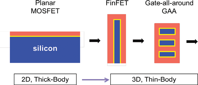
Evolution of transistor structure
Power Consumption, MOSFET, CMOS, Thin-Body CMOS, 3D Transistor: If we want to cramp a hundred times more transistors into a chip of a certain size, we need to reduce the power consumption per transistor by about a hundred times. Otherwise, heat removal would be a nightmare, not to mention the impact of such energy use on mother earth. A major change that reduced power consumption was the transition from bipolar transistors to MOSFET and then CMOS. CMOS technology reduced the standby current of circuits to nothing but the transistor leakage current.
The basic MOSFET structure remained unchanged from 1960 for 50 years until reducing MOSFET size further without degrading leakage, speed or switching energy became impossible. In 2011 Intel adopted the first 3D transistor, FinFET for production. FinFET and the thin-body MOSFET concept arise from the insight that the leakage current basically cannot flow within several nanometers (nm) of the Si surface because the surface potential is well controlled by the gate voltage. In the figure showing the MOSFET evolution, FinFET has a vertical Si fin (in blue), about 10nm thin, as the transistor body. The body is covered by gate oxide (in yellow) and gate metal (in orange) and leaves no Si outside the range of strong gate control. It reduces the leakage current by orders of magnitude. Furthermore, the FinFET size can be reduced every few years as long as the fin thickness is also reduced. Another thin-body MOSFET demonstrated in the same DARPA research project as FinFET is the ultra-thin-body SOI (UTBSOI or FDSOI). Being a 3D transistor, FinFET has a smaller footprint than the planar MOSFET. It has the same advantage as building tall buildings instead of single-story buildings in a crowded city.
The fin of FinFET has become thinner and taller with each new technology node. At the 2nm node, it is too hard to make the required thin and tall fin by lithography and etching. The industry is adopting a new 3D thin-body MOSFET structure called NanoSheet or GAA (gate-all-around), where the thin body is made by epitaxial growth and etch-release. The figure above illustrates the evolution from FinFET to GAAFET.
Examples of What May Happen Next
3D transistors and 3D packaging are here to stay. 3D NAND technology is an excellent example of a cost-effective monolithic 3D memory IC. Monolithic 3D logic IC may start with stacking PFET on top of NFET to reduce CMOS-gates’ footprints. Future monolithic 3D IC paths may employ transferred single-crystal semiconductor films, self-assembled 2D semiconductors, or amorphous or polycrystalline semiconductor films as the transistor material. 0.6nm MoS2 monolayer has been used to demonstrate 1 nm gate-length thin-body MOSFET. Power supply voltage and power consumption may be reduced by many folds with Negative-Capacitance Transistor (NCFET). It requires inserting a thin layer of ferroelectric such as HfZrO in the MOSFET gate stack. Another advantage of adding the thin ferroelectric is its memory property that may be exploited for computing in memory or fast non-volatile memory.
Does the World Need More and Better Transistors?
The enormity of the task of dealing with global warming (see the graph below) is beginning to be realized. What about the task of dealing with the next Ice Age, which is predicted to start in 1500 years based on Earth’s orbit? Humans may need order-of-magnitude greater capabilities to deal with future existential challenges.
But how can we possibly get 10x or more problem-solving power? Electronics are the key. While all technological advances bring forth new capabilities, electronics are unique for three reasons.
1) Its impact is infectious. High-speed communication and computing, automation, internet, AI, robotics, and yet-unknown future technologies enabled by better transistors have lifted and will lift up all technologies, industries, and sciences. And they in turn lift each other.
2) ICs use relatively small amounts of materials. And the less materials they use (by being made smaller), the faster and more capable they become.
3) Theoretically, the energy required for information manipulation can still be reduced by more than a thousand times. Although we have no idea how to get there now, reducing the energy by 10 or 100 times would not violate physical laws. The energy efficiencies of other technologies (transportation, lighting, …) are mostly already around 50% of their theoretical limits.

Variation of global mean temperature
Lesson From the Past and Task for the Future
The history of transistors is a journey log of climbing one hill after another. Until we get high enough on one hill, we can not even see the terrain and map a route to reach the next hill. Importantly, with each hill climbed, we accumulate and discover new skills that help us move forward. Deposit and etch materials one atomic layer at a time? Sure. Economically on millions of wafers every week at high yield with billions of transistors on each chip? Sure. Magnetic, ferroelectric, and optical materials too? Sure. Switch the magnetic polarization with an electric field, not current? Sure. Do anything that does not violate physical laws? Probably. Continuing the hard climbs while diligently scouting for new provisions and possible routes is the best way to create future electronics, which may be very different in devices, materials, and operating mechanisms. The new provisions and route will come from university and industry researchers with deep knowledge in physics, chemistry, biology, and algorithms—and the help of expanding problem-solving capabilities, time, and luck.
Biography

Dr. Hu received his B.S. degree from National Taiwan University, which honored him with its Distinguished Alumni Award, and M.S. and Ph.D. degrees from UC Berkeley. Dr. Chenming Hu is called the Father of 3D Transistors for developing the FinFET in 1999. Intel hailed FinFET as the most radical shift in semiconductor technology in over 50 years. Modern computers, smart phones, and the internet all ran on 3D transistor processors. He received the US National Technology and Innovation Medal from President Obama in 2016. He leads the ongoing development of BSIM, a suite of industry-standard computer models of transistors. University of California provides it royalty free for the global IC industry to design integrated circuits worth well over a trillion US dollars since 1995. IEEE, world’s largest technical professional organization, gave him its highest award, Medal of Honor, in 2020 for helping to “keep Moore’s Law going over many decades’’ after lauding him as “Microelectronics Visionary” for “achievements critical to producing smaller yet more reliable and higher-performance integrated circuits” in 2009. The 2013 Kaufman Award cited his “tremendous career of creativity and innovation that fueled the past four decades of the semiconductor industry”. Dr. Hu is TSMC Distinguished Chair Professor Emeritus of the University of California, Berkeley. From 2001 to 2004 he was the Chief Technology Officer of TSMC, now the world’s largest semiconductor company. He was the board chairman of the nonprofit Friends of Children with Special Needs and the East Bay Chinese School. He has authored six books and 1000 research papers and received over 100 US patents and honorary doctoral degrees from the University of Hong Kong and NYCU in Taiwan. He is honored with memberships in the US National Academy of Engineering, Chinese Academy of Sciences, US Academy of Inventors, The World Academy of Sciences and Academia Sinica. His other professional honors include Asian American Engineer of the Year; Silicon Valley Engineering Hall of Fame; IEEE Jack Morton Award, Solid State Circuits Award, Nishizawa Medal, and the EDS Education Award for “distinguished contributions to education and inspiration of students, practicing engineers and future educators.” He also received UC Berkeley’s highest honor for teaching—the Berkeley Distinguished Teaching Award.