

Technical Briefs
Lithography and Patterning
Introduction
The International Roadmap for Devices and Systems (IRDS) is a roadmap that forecasts progress in both devices and systems. It starts from projecting future performance at a high level and then has sections projecting the future requirements, short- and long-term challenges and discusses key technologies needed to enable the overall roadmap. The lithography and patterning roadmap is a section of the overall roadmap specific to these subjects. Shrinking dimensions through lithography and patterning has always given more devices per unit area of silicon, and this is a key factor in semiconductor progress.
Currently, logic devices have the smallest critical dimension and tightest overlay requirements of any kind of device. The current logic device roadmap from the most recent full More Moore roadmap1 is shown pictorially in Fig. 1. It shows the projected future progression from finFETs to lateral gate all around (LGAA) to complementary n- and p-FETs to 3D stacking of devices.

Figure 1. Device structures in IRDS More Moore Roadmap.
From a lithography and patterning point of view, this device progression has two distinct phases. From 2022 through 2028, devices get more complex and feature sizes shrink. From 2031 to 2037, increased device density is achieved through stacking of devices. In other words, in roughly 8 years logic will switch from scaling by shrinking to scaling by stacking. Fig. 2 shows what this looks like in terms of key dimensions over time. Logic minimum metal half pitch, the smallest critical dimension (CD) in a modern logic device, shrinks to 8 nm in 2028 and then doesn’t shrink anymore after scaling is done by shrinking. Other key logic dimensions, the via half pitch and minimum contact hole CD, follow a similar pattern.
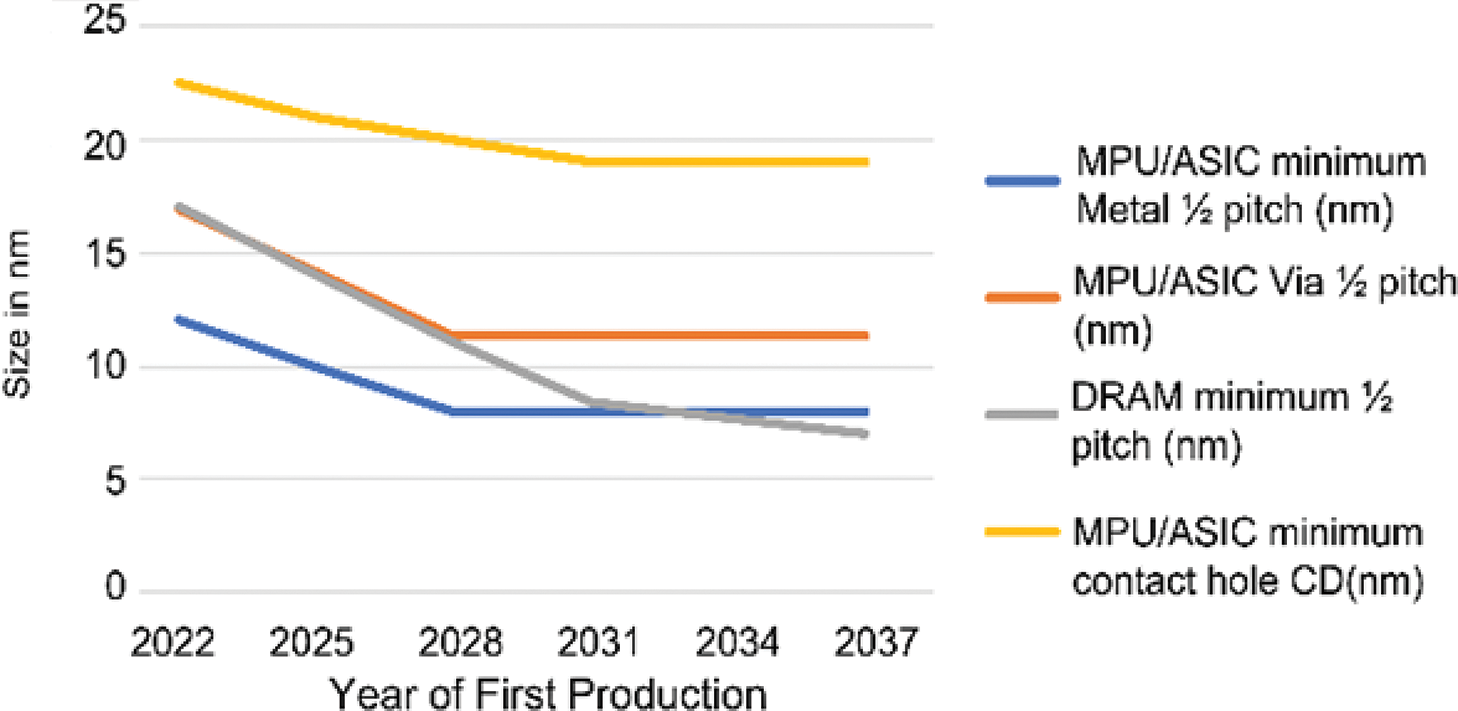
Figure 2. Key leading edge device dimensions over time. Different key dimensions are shown by different colored lines.2
DRAM minimum CDs trail logic, but DRAMs are projected to keep shrinking after 2028 and these dimensions eventually will be smaller than critical logic dimensions. However, it is likely that DRAMs will also switch to stacked devices in the near future because smaller and smaller dimensions make it harder and harder for planar devices to store enough charge for sufficient device performance. Flash memory has already switched to scaling by stacking instead of scaling by shrinking devices. Overall, it is likely that leading-edge devices will all switch to scaling by stacking from scaling by shrinking sometime in the mid-2030s. Thus, the lithography and patterning roadmap has two phases. First, leading-edge devices will shrink dimensions to get more and more devices per unit area. Then, scaling will change to creating stacks of devices to get more devices per unit area. These two phases have different lithography and patterning challenges.
Scaling by Shrinking
Leading-edge integrated circuit manufacturing today, with half-pitch ≤ 12 nm, uses extreme ultraviolet (EUV) lithography. First employed for manufacturing in 2019, it uses a wavelength of 13.5 nm, fourteen times smaller than the smallest wavelength previously used in production, 193 nm. Current EUV tools print features more than three times smaller than 193 nm lithography can. EUV exposure tools are large and expensive. The EUV exposure tools used currently in manufacturing weigh approximately 180 tons, have 100,000 precision parts, and cost well over 100 million dollars.3 Future generation of EUV exposure tools will be even more massive and expensive.
This name EUV sounds like you are using an optical wavelength, but the actual wavelength is 13.5 nm, which is a kind of soft X-ray. The differences between traditional optical lithography and EUV were big challenges to overcome in making EUV work. Unlike optical wavelengths, atoms absorb EUV radiation, not chemical functional groups. Everything absorbs EUV, including air, so the entire optical train must be in a vacuum and refractive lenses are impossible to make. EUV lenses are made from mirrors and EUV masks are mirrors with patterns of absorber on top. The wavelength of 13.5 nm was selected because mirrors could be made that worked at this wavelength. The mirrors are made from many alternating layers of molybdenum and silicon of precise thickness, and they reflect a maximum of roughly 65% of the incident light. Because multiple mirrors make up the lens and the illuminator, a lot of light is absorbed in the optical train and bright sources of light are required to produce enough light to reach the wafer surface. Light sources had to be invented in order to have enough light for exposure, and this challenge was a source of many delays in bringing EUV to manufacturing capability. Current tools used in production have light sources rated at 500 W. Because of the loss of light at each reflection, only approximately 1% of this light reaches the wafer. Thus, the throughput of the tool is usually constrained by the photo speed of the resist and this affects the cost of each exposure. As discussed below, photoresists in the future will require higher exposure doses to control stochastic effects. This will require much brighter light sources and/or improved optical paths with less light loss in order to expose wafers with desirable throughputs. This is a major challenge to accomplish.
The numerical aperture (NA) is a numerical description of what angles of light diffracted from the mask can be collected by the lens and imaged on the wafer. Higher NA gives higher resolution but worse depth-of-focus (DOF), that is, smaller features can be printed, at the expense of greater difficulties in controlling linewidth variation. The EUV exposure tools used in manufacturing today have NA = 0.33, while tools with NA = 0.55 have recently started to be shipped to customers. The increased NA will reduce the theoretical minimum printed size by 40% and the theoretical DOF by 64%. This reduced DOF is a key challenge of high-NA EUV lithography. Not only must all the mechanical tolerances inside the exposure tool be improved, but also some new factors that affect the total defocus window become important. For example, because of the complex interactions of EUV light with the masks, there are differences in the best focus positions for lines of different pitches. This will affect the total defocus window. The lack of a large focus window will force thinner films of photoresist. Thinner films of resist will make pattern transfer difficult and, as discussed below, make it harder to address stochastic effects.
The reflective optics in EUV exposure tools forced compromises in high NA tool design. EUV lens design requires that light illuminating the mask comes from an angle away from the vertical so that the light isn’t reflected back into the light source. The middle of the angular illumination spread at the mask in a 0.33 NA tool is six degrees. The range of angles illuminating the mask scales with the NA. However, this range can’t be made arbitrarily large because the mask reflectivity will decrease too much (see Fig. 3). The range of angles illuminating the mask can be reduced by making a lens with a higher demagnification factor, but this reduces the field size that can be printed in one exposure. The 0.55 NA tools now being introduced have anamorphic lenses, where the magnification factor is different in the x direction than in the y direction. In these tools, the magnification factor is 8× in one direction and 4× in the other direction. This reduces the exposure field size in half from a maximum of 858 mm2 to 429 mm2, which is much better than the 4× field size reduction that a full 8× magnification factor would require.
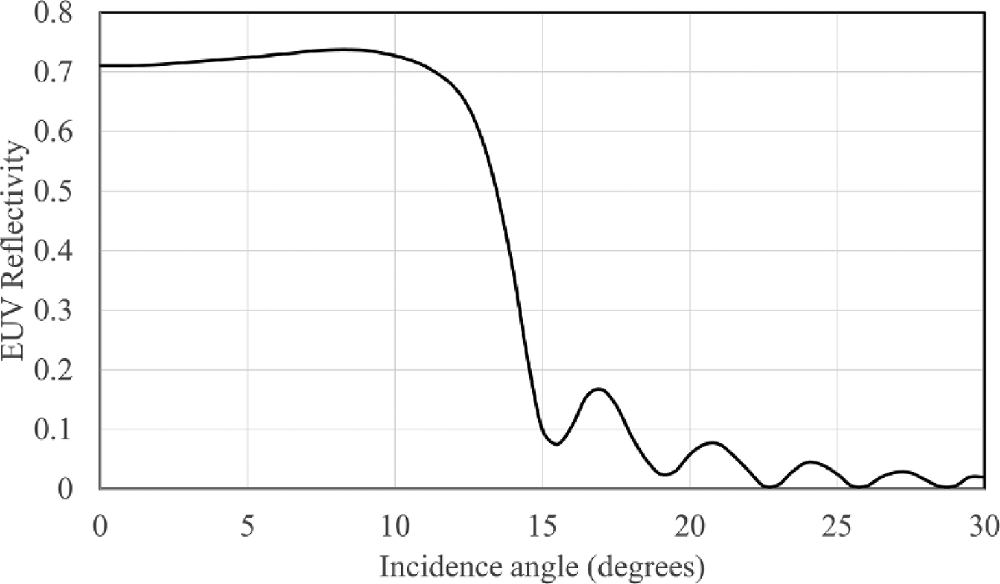
Figure 3. Calculated reflectivity from a Mo/Si mirror as a function of angle.4
Even higher NAs than 0.55 are conceivable and are considered “hyper-NA EUV”. Such tools would be larger, more complicated, and have even less DOF. Also, as the NA increases, the contrast of images created with unpolarized illumination decreases, and polarized illumination is preferable. However, polarization is difficult to accomplish with current EUV light sources and would result in the loss of over half the light. This would put even more pressure on developing high-brightness or light sources that use different technology. A free electron laser (FEL) is such a different, high-power light source that generates polarized EUV light. FELs are very large, but a single FEL could provide light for tens of exposure tools. FELs for use as a source of light for EUV lithography are currently being developed.5
Statistical variation (often referred to as ”stochastics”) is a major challenge for printing smaller features. For example, a given exposure dose of light, even if perfectly controlled for energy, will have random quantum fluctuations in the number of photons from feature to feature and from exposure to exposure. This variation, as a percentage of exposure dose, gets larger as the number of photons in a dose gets smaller. For the wavelength of light generated by ArF lasers (193 nm) and larger wavelengths, this variation, known as photon shot noise, is insignificant, but for EUV it is quite significant, especially for high-speed resists where there are fewer photons per exposure dose. Chemical inhomogeneity at the molecular level is also a contributor to stochastic variations, and it is currently comparable to shot noise. The chemical noise comes from random variations in the positions and number of resist components, random variations in light absorption, and from electron trajectories. The electrons are generated after absorption of EUV light and are what induces the chemical changes in the exposed areas of the resist.
These stochastic effects cause random variations in the positions of the edges of features. Lines have rough edges, giving line edge roughness (LER) and line width roughness (LWR) and contact holes have random variations in size. LER affects device performance and was already an issue for 193 nm lithography. For EUV, it is a bigger issue because the features are smaller, the numbers of photons in exposure doses are smaller and the numbers of molecules in a typical feature are also smaller. These effects can be improved by using slower photoresists, but of course slower resists reduce throughput and increase costs. In practice, EUV users will pick the fastest resist that meets LER and related requirements. Because the numbers of photons and numbers of molecules per feature go down as feature sizes get smaller, resist photospeeds will need to be slower as feature sizes get smaller. The estimate for hole type features from the 2022 IRDS is shown graphically in Fig. 4.
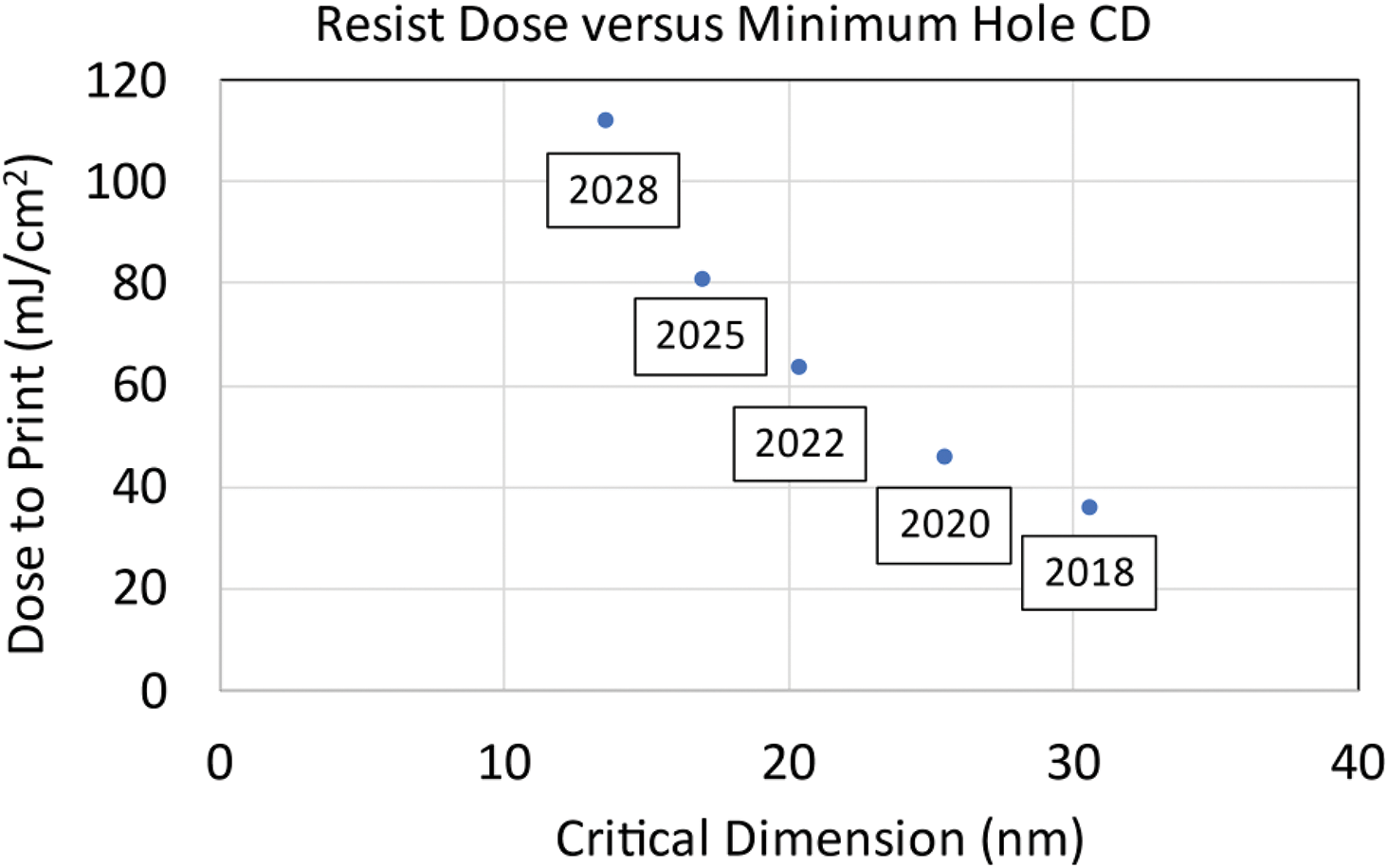
Figure 4. Estimated dose-to-print for leading contact holes printed with EUV.
This dose-to-print projection assumes significant improvements in resist and imaging even to meet these projected photospeeds. Obtaining these improvements is a significant challenge, especially as resist films are expected to get thinner for each successive node. Even though basically everything absorbs EUV radiation, thin films of resist often absorb a less-than-optimum amount of EUV light. Lower light absorption means fewer photo events per volume which results in worse stochastics. For EUV, unlike other wavelengths in use, formulators try to get enough light absorption rather than avoid too much light absorption.
Resist processes often involve the diffusion of photoproducts, which can effectively blur images. Resists optimized for smaller feature sizes require less blur. Blur is a measure of how much resist volume is affected by a single photoevent. A large value of blur gives a faster photospeed, all other things being equal. But too big a blur will reduce the process window of a resist. For example, if the printed dimension reduces from 12 to 10 nm and the resist blur is reduced proportionally to maintain a good resist process window, the amount of chemical change per photo event will decrease by 43%. This is a large increase in the dose to print. Resist developers will have to make resist chemistry more efficient and more absorbent node-to-node to compensate for this effect and match the values shown in Fig. 4. Even with the improvements assumed in Fig. 4, the source powers and/or the efficiency of the optical train of EUV tools will have to increase.
Another path to smaller features involves using multiple patterning. Multiple patterning was developed to enable the patterning of smaller features than could be printed in one exposure with 193 nm immersion lithography. It involves more than one exposure per layer and many processing steps to create patterns with a smaller pitch than a single printed pattern. The process complexity and resulting long process development cycles of multiple patterning are drawbacks, but its ability to provide dimensions below optical resolution limits makes it one of the most powerful resolution enhancement techniques ever introduced. Double patterning and its extension quadruple patterning are still used despite the present availability of EUV lithography and will continue to be used where appropriate. Fig. 5 is from the 2022 IRDS roadmap and shows potential patterning solutions for critical levels of future nodes. Depending on cost and pattern type solutions, multiple patterning with 0.33 NA EUV and single patterning with 0.55 NA are both possibilities for these levels. In all likelihood, both will be used in the future.
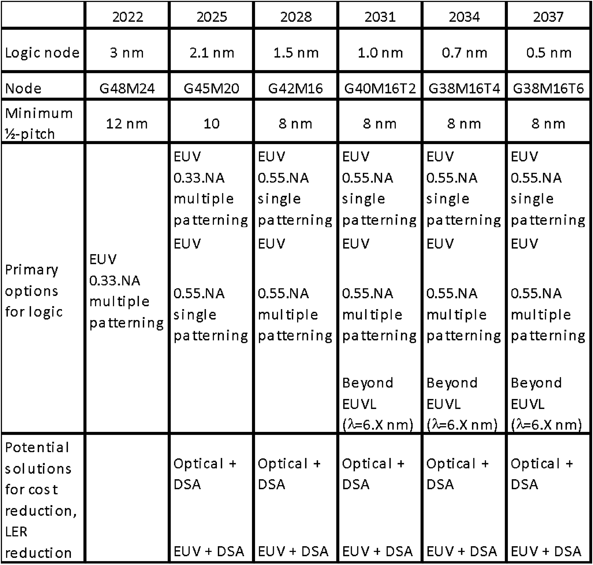
Figure 5. Potential Solutions for Leading-Edge Logic Lithography (DSA - Directed Self-Assembly).
Scaling by Stacking
The roadmap in Fig. 1 shows that around 2031 scaling of logic devices will change to stacking devices on top of each other and, as shown in Fig. 2, the minimum dimensions will stop shrinking from node to node. This is driven by device functional considerations. Electrical considerations such as leakage, impedance, and other factors make it a challenge to keep shrinking devices and have them work well. It’s possible that clever design can change the time frame for the introduction of stacked devices, but there is no doubt that stacking will give more devices per area, which is always desirable. The current roadmap projects that this transition will occur when minimum CDs reach 8 nm half pitch. As shown in Fig. 5, the introduction of 0.55 NA EUV tools will make this printed dimension printable either by single or double patterning. The IRDS estimates that the number of critical levels imaged by EUV will multiply with the number of tiers of devices resulting in many more critical EUV levels per wafer. It is likely that these critical levels will contribute to most or all of the defects found in mature manufacturing processes. The IRDS More Moore roadmap projects required defect levels for logic devices. These defect levels can be used to calculate how much relative EUV defectivity needs to improve (Fig. 6). For the first two node changes shown, defectivity has to improve by roughly the amount of CD shrink from node to node. This matches historical experience and should be a normal technology extension to achieve. But once scaling switches to stacking, defectivity has to improve by an order of magnitude every node. This is a major challenge. Even if better EUV tools and processes aren’t needed for resolution, they will be needed to make patterning more reliable.
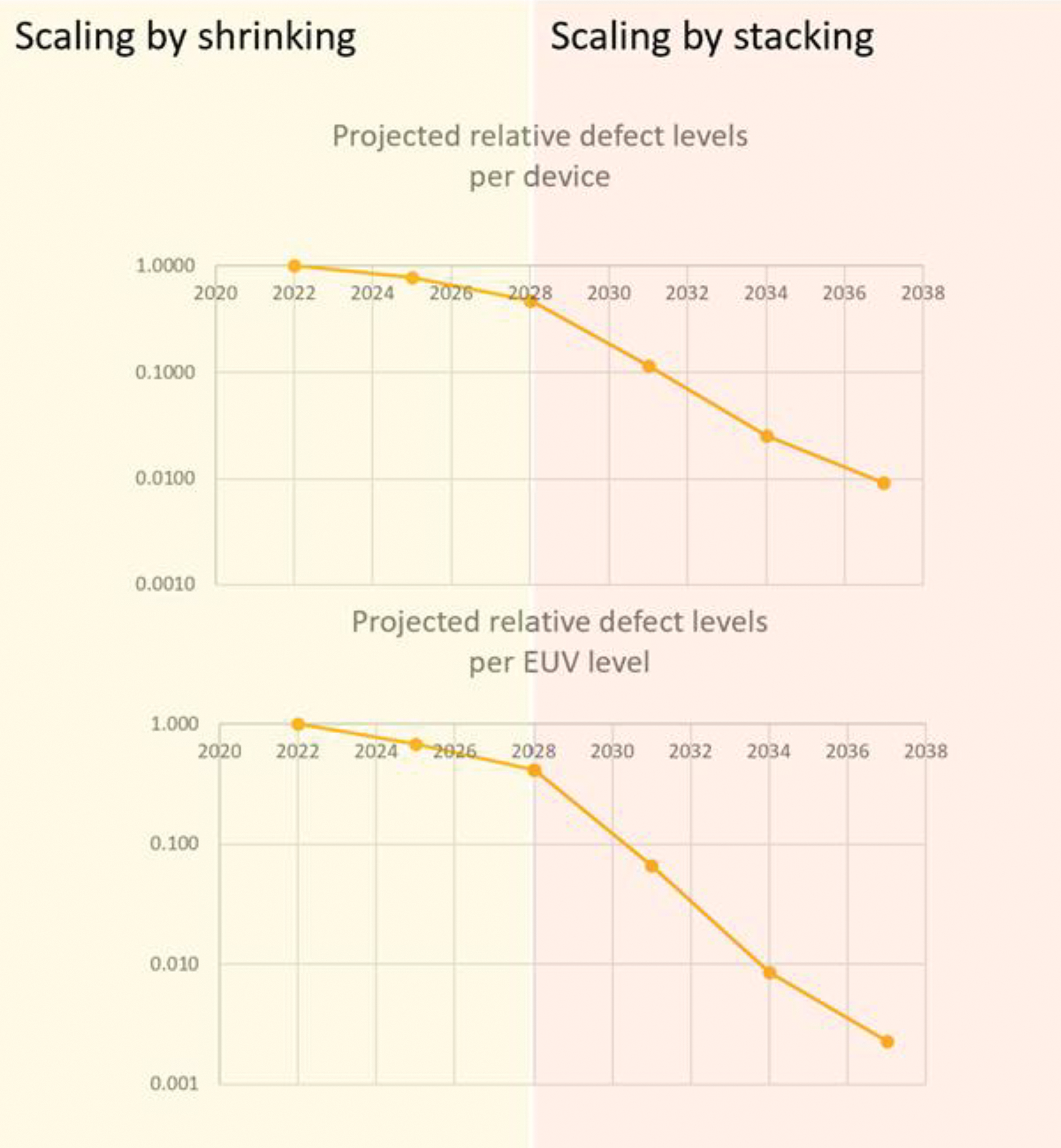
Figure 6. Lithographic defect requirements per node shown on a relative scale for both defects per device and defects per EUV level.6
Even without these stringent defectivity targets, EUV already has defect worries due to stochastic issues. Line width variation due to stochastics is typically characterized by the mean width and the standard deviation of that width and this standard deviation is used to specify LER, LWR, and a critical dimension uniformity (CDU). The width distribution appears normal (Gaussian) when widths within several sigmas are measured, but when much larger samples are measured (going out to tens of millions of samples) the distribution is not normal at all.7,8 Randomly closed or bridged contact holes and randomly bridged or broken lines can appear. The frequency of these defects depends on many factors, but some factors are already clear. Underexposure or overexposure increases the stochastic defect rate, so there is a size window for printed features where the defect rates are acceptable. If the defect rate target is too small, there will be no printed size at which there are no defects. Current measured defect rates for model systems can be large compared to the billions of features in current high-performance chips. Ensuring low defectivity in the future is a major challenge.
Per chip defectivity has a strong dependence on chip size, so smaller chips can help with this. And smaller chips match high NA tool sizes. However, creating complex systems with smaller chips requires integrating many small chips. This approach is called using chiplets.9 Not all circuit elements shrink node-to-node. Digital elements, such as logic and memory cells, benefit from shrinking dimensions from node to node. But analog elements, such as input/output structures, are tied to external physical requirements that do not scale strongly node-to-node. An advantage of the chiplet approach is that only high-performance digital elements need to be made with the highest performance technology. However, integration of many chiplets in a package requires high-performance, dense connection elements. Advanced packaging can have system performance benefits, such as improved communication between logic and memory.10 This advanced packaging has its own lithography requirements. Packaging substrates can have different form factors than standard silicon wafers, and packages may cover areas larger than the common 26 mm x 33 mm exposure field size. To avoid the use of many reticles and stitching, exposure tools need to have large exposure field sizes. Direct write lithography could be beneficial in this regard. Moreover, in some packaging processes, chiplets are attached mechanically to substrates and interconnects need to be made between features that have been placed imprecisely. Following metrology, direct write lithography could be used to adjust the placement of packaging interconnects to match those of the mechanically placed features.
Besides the resist challenges discussed above, new patterning methods are needed in order to improve edge placement errors. By optimizing device design and technology at the same time, the area of a device unit cell can shrink faster than the scaling of dimensions alone would suggest. Self-aligned technologies, such as self-aligned blocks and fully self-aligned vias, improve edge placement errors (EPE) and enable denser device designs. However, as devices continue to scale, better materials with lower dielectric constants will be needed for these structures. When scaling switches to stacking, these challenges will be even more important.
Conclusion
The IRDS roadmap predicts that logic devices will have the smallest dimensions of production chips and will continue to shrink node-to-node until 2031, after which more devices per unit area will be achieved by stacking instead of by shrinking. Shrinking of device dimensions will require improvements in EUV lithography, particularly using higher NA tools. These improvements will give better resolution but make controlling line width variation more difficult, both because of smaller DOF and greater stochastic effects. Stochastic effects are random fluctuations in photon numbers and in the positions and numbers of different molecules in photoresists. These effects cause variations in the size and shape of printed features. Even with substantial improvement in tools and materials, controlling these effects will require using slower photoresists and increase the cost of EUV. Multiple patterning will be used along with higher NA EUV to provide multiple options for shrinking feature sizes. New materials will be needed for self-aligned structures in order to ensure that smaller structures meet performance targets.
Higher NA tools have smaller exposure field sizes, making it harder and more expensive to produce the large area chips preferred for some applications. This may result in increased use of chiplets along with advanced packaging, where many smaller chips are connected with packaging that gives enough high-performance electrical connections to maintain a high system performance overall. When scaling changes to stacking, the defect rate per EUV level will have to improve by an order of magnitude for each node. This will pose new challenges to lithography even though the minimum chip dimensions aren’t shrinking.
Endnotes
1 Available at https://irds.ieee.org/editions/2022/more-moore by free download
2 These dimensions are available in the 2022 Lithography roadmap, https://irds.ieee.org/editions/2022/irds%E2%84%A2-2022-lithography
3 https://www.ed.nl/asml/asml-heeft-nieuwe-megahal-hard-nodig~aa0c87ee/
4 Obert Wood II, Keith Wong, Valentin Parks, Patrick Kearney, Julia Meyer-Ilse, Vu Luong, Vicky Philipsen, et al., “Improved Ru/Si multilayer reflective coatings for advanced extreme-ultraviolet lithography photomasks.” Proc. SPIE 9776, Extreme Ultraviolet (EUV) Lithography VII, 977619 (18 March 2016); https://doi.org/10.1117/12.2219215
5 Erik Hosler and Chris Anderson, “The last light source,” presented at SPIE Advanced Lithography + Patterning Symposium, 25–29 February 2024
6 See the 2023 IRDS Lithography and Patterning update at https://irds.ieee.org/editions/2023/irds%E2%84%A2-2023-lithography
7 Timothy A. Brunner, Xuemei Chen, Allen Gabor, Craig Higgins, Lei Sun, and Chris A. Mack, “Line-edge roughness performance targets for EUV lithography,” Proc. SPIE 10143, Extreme Ultraviolet (EUV) Lithography VIII, 101430E (24 March 2017); https://doi.org/10.1117/12.2258660
8 Robert L. Bristol and Marie E. Krysak, “Lithographic stochastics: beyond 3σ,” Journal of Micro/Nanolithography, MEMS, and MOEMS 16(2), 023505 (12 June 2017), https://doi.org/10.1117/1.JMM.16.2.023505
9 Harry J. Levinson, “Technological innovations for a sustainable business model in the semiconductor industry”, Proc. SPIE 9189, Photonic Innovations and Solutions for Complex Environments and Systems (PISCES) II, 91890E (5 September 2014); https://doi.org/10.1117/12.2060976
10 Philip Jacob, Aamir Zia, Okan Erdogan, Paul M. Belemjian, Jin-Woo Kim, Michael Chu, Russell P. Kraft, John F. McDonald, and Kerry Bernstein, “Mitigating memory wall effects in high-clock-rate and multicore CMOS 3-D processor memory stacks.” Proceedings of the IEEE, 97, no. 1 (2009), 108-122, https://doi.org/10.1109/JPROC.2008.2007472
Your comments are most welcome. Please write directly to the Editor-in-Chief of the Newsletter at
daniel.tomaszewski@imif.lukasiewicz.gov.pl
 |
 |
The 36th IEEE International Conference on Microelectronic Test Structures
The 36th IEEE International Conference on Microelectronic Test Structures took place in Edinburgh between the 15 and 18 April 2024, hosted by the University of Edinburgh and sponsored by the IEEE Electron Devices Society. The venue for the conference was the University’s South Hall Complex in the shadow of Arthur’s Seat. In addition to the technical and tutorial sessions, the conference included an equipment exhibition with contributions from sponsors including: Advantest Corporation, Suzhou Eoulu System Integration Co. Ltd., Celadon Systems Inc., FormFactor Inc., Keysight Technologies, MPI Corporation, and HProbe. We would like to thank them for their support for the conference.
The conference began with a one-day tutorial which offered six presentations to the attendees, covering a broad range of topics from test structure fundamentals, via Capacitive micromachined ultrasonic transducers (CMUT) and MEMristors to RF characterization and eventually Photonic devices.
At the opening of the tutorial session, Prof. Yoshio Mita (University of Tokyo) took us on a journey through test structure fundamentals, in which the importance of using test structures was emphasized: “door meten tot weten” (En: “through measuring to knowing”). Next Prof. Daniel Alquier (Université de Tours) provided us with an extensive overview of interesting CMUT technologies, ranging from materials and processes to applications. Memristive Technologies were thoroughly discussed by Prof. Themis Prodromakis (University of Edinburgh), covering testing, modeling, and applications. Dr. Elisa Vianello (CEA Leti) followed by discussing the multifaceted impact of resistive memories on neuromorphic Systems. Dr. Andrej Rumiantsev (MPI Corporation) provided the attendees with a very thorough overview of the fundamentals of accurate wafer-level characterization at the RF and mm-Wave frequencies. The tutorial session was finished by a relatively new, emerging topic presented by Dr. Alexandru Romanescu (SMART Photonics). He provided a thorough overview of devices of photonic integrated circuits, ranging from characterization to test.
Attendees of the 2024 technical session were able to experience technical papers ranging over a wide set of topics organized in sessions named: Layout Dependent Effects; Reliability; Cryogenic Characterization; Ferroelectrics and Dielectrics; MEMs and Sensors; Wafer Measurements; S-Parameters and De-Embedding; GaN Technology; Process/Material Monitoring.
Furthermore, the Conference offered the audience the opportunity to attend four invited presentations, given by experts in the field of experimental characterization and test structures for semiconductor device/process monitoring.
The first invited talk was by Prof. Pete Loftus, Royal Academy of Engineering Visiting Professor of Instrumentation, Applied Metrology & Sensing at The University of Edinburgh. The presentation was entitled “What do we mean by measurement and can we trust it? - A commentary on the application of measurement process and its association with “truth” and gave an overview of over 40 years of Prof. Loftus’ working on different aspects of measurement to take a step back from the applications and to consider measurement itself - what it is, why we do it, and whether we can trust it.
In the second invited talk, entitled “Characterization of ferroelectric HfOx-based devices – methods and test structures”, Dr. Stefan Slesazeck, from NaMLab in Germany, discussed the specific requirements for the characterization of ferroelectric-based devices and for the design of their corresponding test structures.
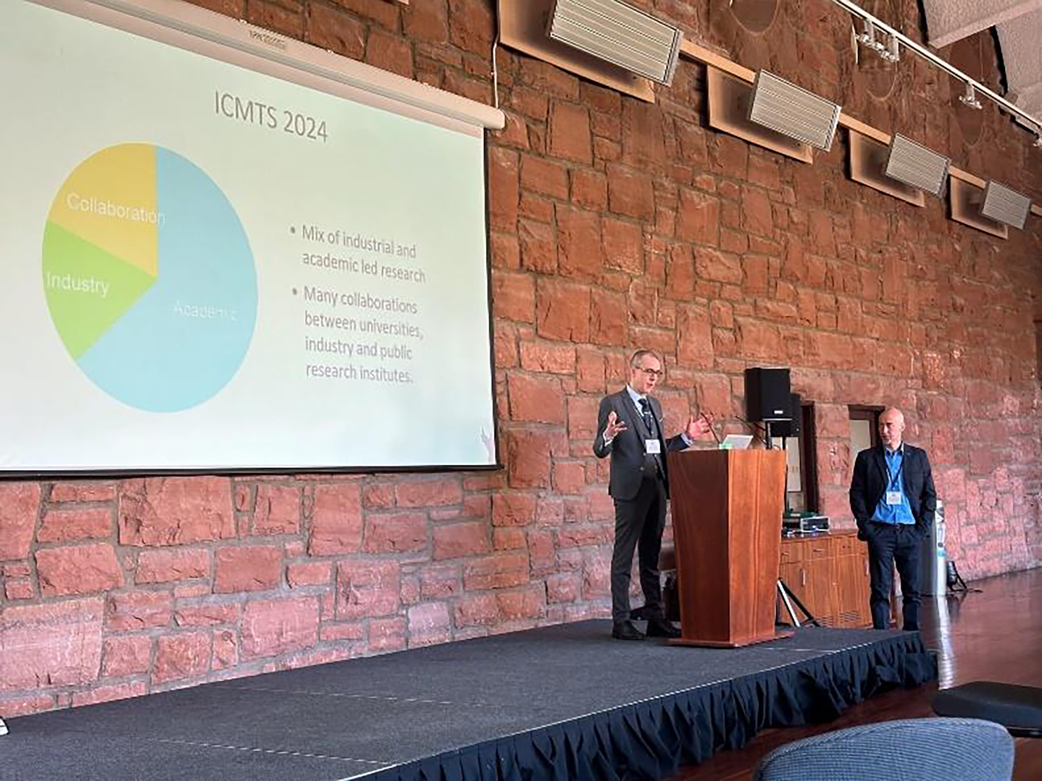
Conference General Chair Stewart Smith (University of Edinburgh) at the podium during the conference introduction, with Technical Program Chair Francesco Driussi (University of Udine).
The third invited talk was given by Dr. Veda Sandeep Nagaraja, from Tyndall National Institute in Ireland who presented “Empowering MEMS Innovation: Bridging Access through EU Access Programmes”. The talk introduced the PiezoMEMs studied at Tyndall National Institute, linked to areas including space technology, communication systems, and packaging. The talk also gave an insight into three EU Infrastructure access programs, namely EUROPRACTICE, ASCENT+, and INFRACHIP.
The last invited presentation, given by Mr. Michele Stucchi, from imec in Belgium, was entitled “3D interconnects characterization: basic test structures and electrical measurement” and presented examples of 3D interconnect test structures and their relative measurement methodologies, highlighting their important role for 3D technology optimization.
The Technical Programme of the Conference included 30 high-standard contributed papers, selected after the peer review by the Technical Program Committee (TPC). A number of noteworthy papers are highlighted here, in particular those that vied for the coveted best paper award. This year, the TPC awarded the prize to the paper presented by L. Pirro and coworkers, from GlobalFoundries and Fraunhofer-IPMS in Germany, entitled “Efficient Characterization Methodology for Low-Frequency Noise Monitoring”. The work proposes a novel methodology for Low-Frequency Noise (LFN) characterization on large device statistics, that relies on the measurement and modeling of the maximum drain current fluctuations over time, see Fig. 1. The approach was validated over different transistor geometries, gate oxide thicknesses, and characterization temperatures, demonstrating how it is possible to evaluate different process integration elements with an automated procedure that is much faster than the classical LFN measurement.
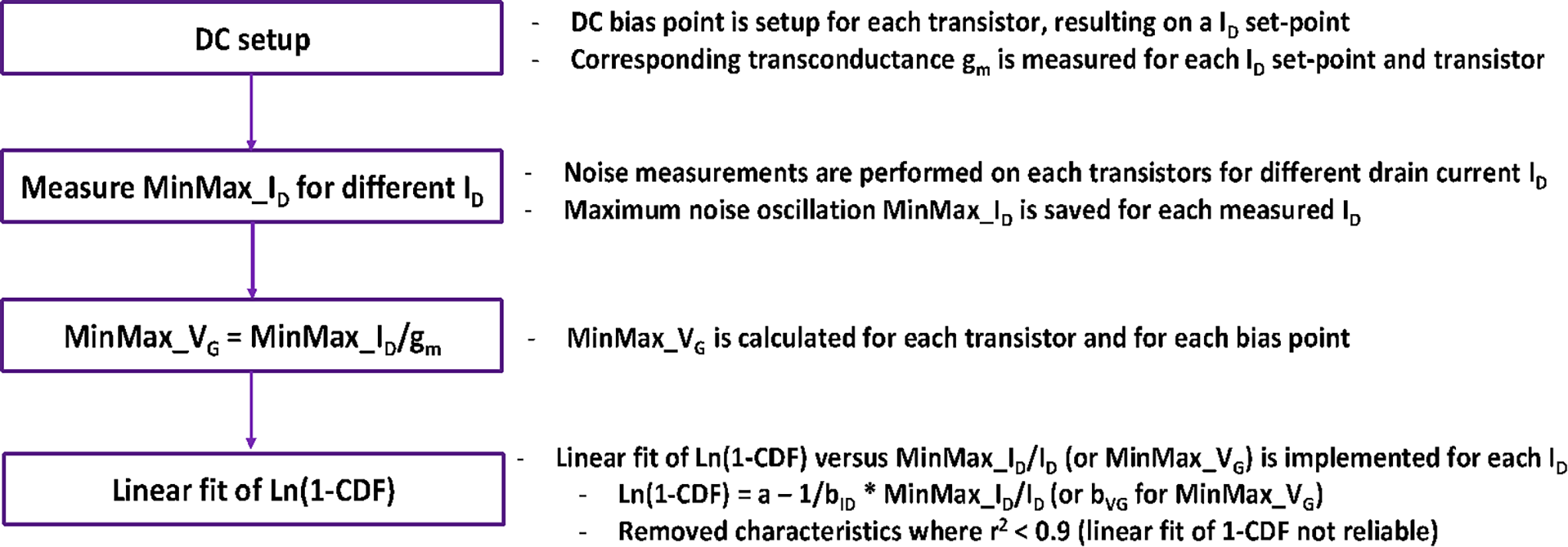
Figure 1. Flow chart of the Low-Frequency Noise (LFN) characterization methodology with associated explanations of key steps.
Another presentation that caught the attention of the attendees was given by Oliver Dieball of NXP Semiconductors in the Netherlands. In the broader context of packaging-induced stress effects, the paper entitled “Test Structures for Studying the Impact of the Backend Contact Metallization on the Performance and Stress Sensitivity of SiGe HBTs” assessed the individual impact of metallization layers above the base, emitter, and collector regions of heterojunction bipolar transistors (HBT), see Fig. 2. The work demonstrated how the HBT collector current largely depends on the metallization layouts, but also on the operating temperature. Finally, metal stacks covering devices do not absorb stress but in fact increase the sensitivity of a device to externally applied out-of-plane mechanical stress.
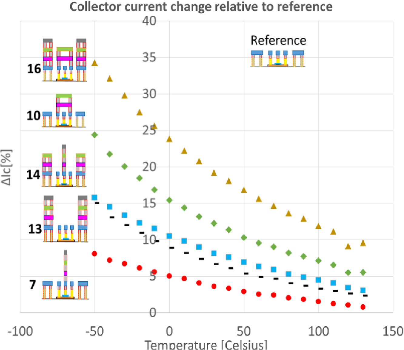
Figure 2. Change of the collector current evaluated at VBE = 0.65 V relative to the reference structure as a function of temperature. The largest impact at low temperatures is introduced by the metallization above the base and the collector regions. As the temperature is increased additional mechanical stress from the backend partially relaxes and the relative differences become smaller.
In the field of ferroelectric-based devices, the paper entitled “Analysis and Compensation of the Series Resistance Effects on the Characteristics of Ferroelectric Capacitors” by Marco Massarotto and coauthors, from the University of Udine (Italy) and NaMLab (Germany), assessed the impact of unwanted series resistances on the switching dynamics of Ferroelectric test structures. In the literature, such an effect has been often overlooked, interpreting the distortions observed in the measured current-voltage (I-V) and polarization-voltage (P-V) hysteresis loops of the ferroelectrics as a signature of the switching speed limit of the material. This work finally clarified how also small series resistances may largely affect the device experimental characteristics and proposed a compensation procedure that can be of fundamental importance to discriminate between intrinsic and extrinsic effects limiting the ferroelectric switching dynamics, see Fig. 3.
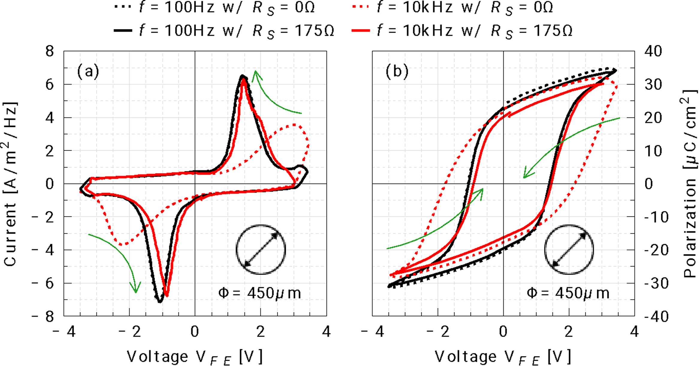
Figure 3. Current-voltage (I-V, a) and polarization-voltage (P-V, b) characteristics measured for two frequencies (f, color). Assuming no series resistances, RS = 0 Ω, the original, non-corrected characteristics (dashed) show deformations at large f, while compensating for RS = 175 Ω, the procedure yields the corrected curves (solid lines), leading to unique I-V and P-V curves, irrespective of f.
In the area of test structures for device reliability studies, a highlight was the paper by Kalid Alkema and coworkers, from STMicroelectronics and Aix-Marseille University in France, entitled “A novel test structure with two active areas for eNVM reliability studies”. The talk presented a new Test Structure with Two Active areas (TSTA) architecture to study the reliability of the eSTM™ cell of STMicroelectronics, see Fig. 4. In particular, the TSTA is able to separate the oxide degradation effects due to programming and erasing operation, respectively. The presented results showed how the Source-Side Injection is mainly responsible for the trapping in the oxide, while the FN erase causes interface states. In principle, the TSTA scheme is also suitable to study the reliability of other non-volatile memories.
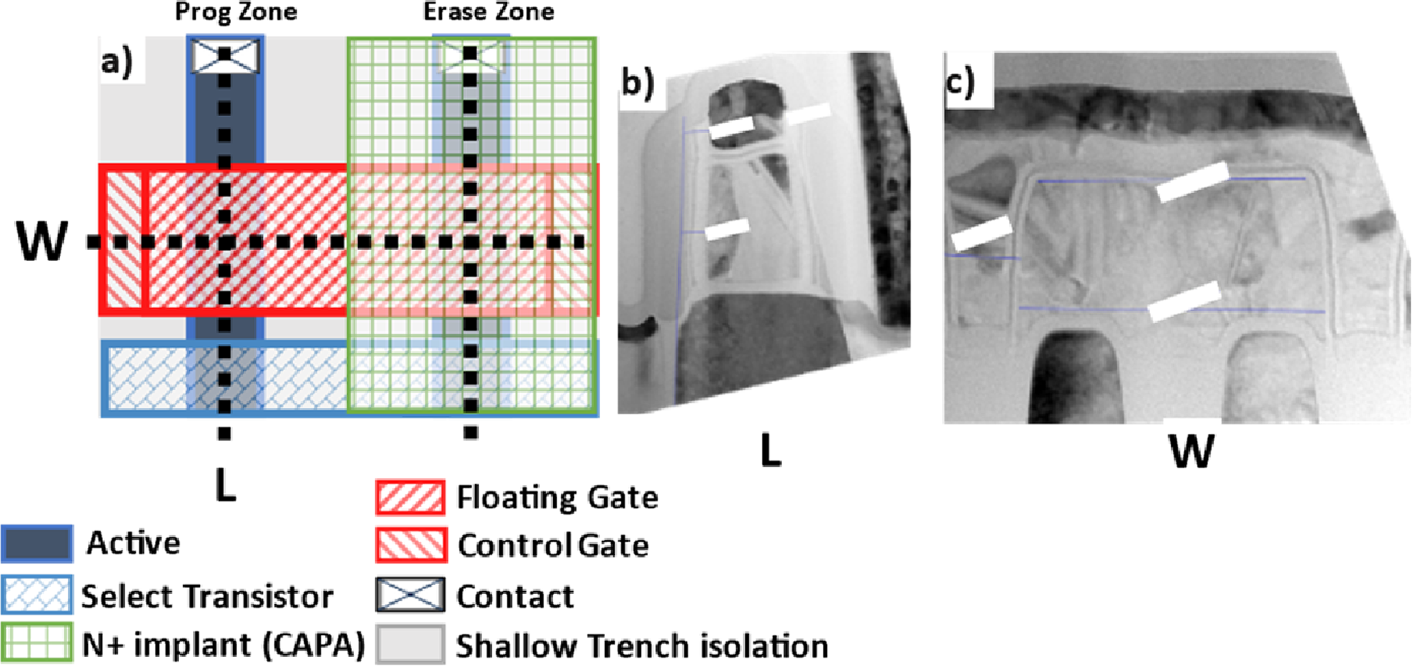
Figure 4. (a) Layout of the Test Structure with Two Active areas (TSTA) architecture to study the eSTM™ cell. (b, c) TEM cuts of the TSTA cell along the width and length.
Other highlights include a paper from Luke Lu and co-authors, from NXP and TSMC, entitled “A Step-by-Step Layout Transformation Approach to Differentiate How Multiple Layout Dependent Effects Modify Device and Circuit Performance”, in which a series of test structures, which step-by-step transformed a Ring Oscillator (RO) layout into single-device modeling layouts, was used to differentiate and quantify the impact of individual layout dependent effects (LDEs) on device DC performance. The findings revealed that the active tiling and well proximity effects are predominant, confirming that the LDEs impact can be decouplable but complicated and they should be carefully considered in design-technology co-optimization.
The Technical Programme Chair for ICMTS 2024, Prof. Francesco Driussi, from the University of Udine in Italy, underlined how the manuscripts presented in this ICMTS edition demonstrated once again the vitality of the semiconductor community in the field of test structures and characterization. Furthermore, the spread of the original works on so many research fields, like process monitoring, characterization of new devices and materials, and design of new sensors and circuits, confirmed the key role of test structures, not only for the yield and reliability monitoring of established technologies but also for the development of the emerging unconventional devices and circuits, keeping the ICMTS Conference of fundamental relevance for the semiconductor industry.
On behalf of all those involved in ICMTS 2024, we would like to thank all attendees for their support and engagement with the conference this year. We hope to see them and others at the next ICMTS conference, planned to take place in San Antonio, TX, USA March 24-27, 2025. The Call for Papers for ICTMS 2025 should be available on the website https://icmts.net
Stewart Smith
General Chair of ICMTS 2024
Francesco Driussi
Technical Chair of ICMTS 2024
 |
 |
 |
 |
2024 IEEE International Memory Workshop (IMW)
The 16th International Memory Workshop (IMW) took place at the Walkerhill Hotel in Seoul, South Korea, from 12–15 May 2024. After the first full in-person 2023 edition held in Monterey which still had reduced participation because of post-COVID issues and a downturn in the semiconductor memory industry, this year’s IMW was the first on-site only after the Covid pandemic with full participation.
The IMW is sponsored by the IEEE Electron Devices Society and meets annually in May. The workshop is a unique forum for specialists in all aspects of semiconductor memories (non-volatile & volatile). The scope of workshop content ranges from new memory concepts in early research to the technology drivers currently in volume production as well as emerging technologies in development. The technical sessions are organized in a manner that provides ample time for informal exchanges amongst presenters and attendees. More than 340 people took part in our meeting this year.
This year’s program included a one-day short course, with tutorials on Advanced Memory and on Neuromorphic Computing, delivered by experts on the topics from both the industry and the academia. The technical program for the single-track conference spanned three days and opened with keynote talks by Kwi Wook Kim (SK Hynix) on “Present and Future, Challenges of High Bandwidth Memories”, Daewon Ha (Samsung) on “Exploring Innovative IGZO-based DRAM Cell Architectures and Key Technologies for Sub-10nm Node”, and Ryota Katsumata (Kioxia) on “Flash memory revolution: journey from 2D to 3D, migrating to modular memory fabrication”
The program included invited talks given by experts in the memory field: Shimeng Yu (Georgia Tech), “Engineering nvCap From FEOL to BEOL with Ferroelectric Small-signal Non-destructive Read”, Andy Hsu (NEO semiconductor), “3D X-DRAM: A novel 3D NAND-like DRAM cell and TCAD simulations”, Hiroko Inoue (SEL), “Heterogeneous OS-FETs Comprising Planar FET and Vertical Channel FETs Monolithically Stacked on Si CMOS, Enabling 1-Mbit 3D DRAM”, Xi-Wei Lin (Synopsys) “Device and Process Simulations for Memory Technology Exploration and Development”, Sven Beyer (GlobalFoundries) “Charge trapping challenges of CMOS embedded complementary FeFETs”, Ashonita Chavan (Micron Technology) “Materials Engineering for High Performance and High Endurance Ferroelectric Memory”, and Gaurav Mehta (Applied Materials) “D2W Hybrid Bonding Challenges for HBM”, each of them providing an exciting overview of the main trends for memory technologies and applications.
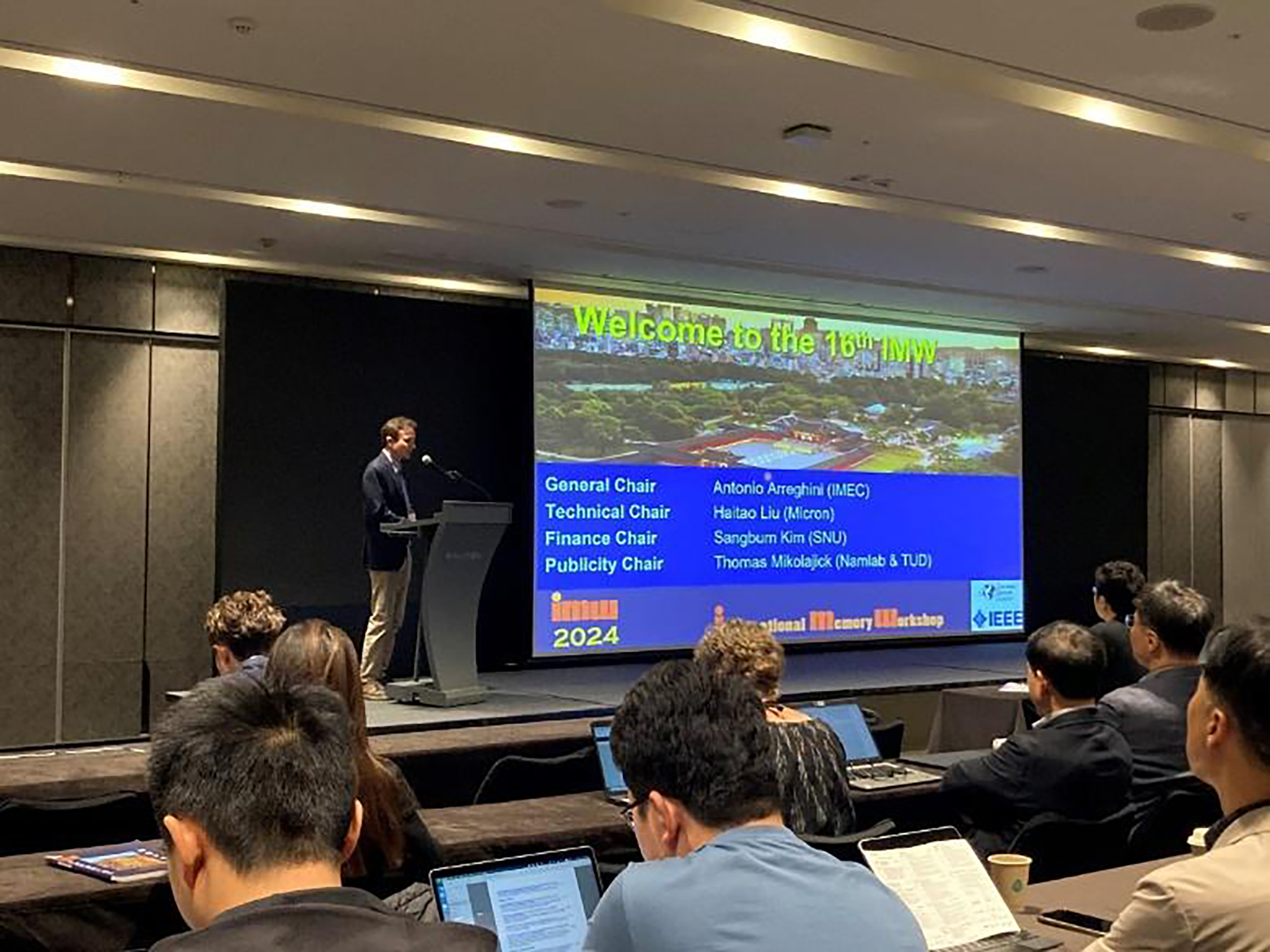
Antonio Arreghini, General Chair 2024, opening the conference.
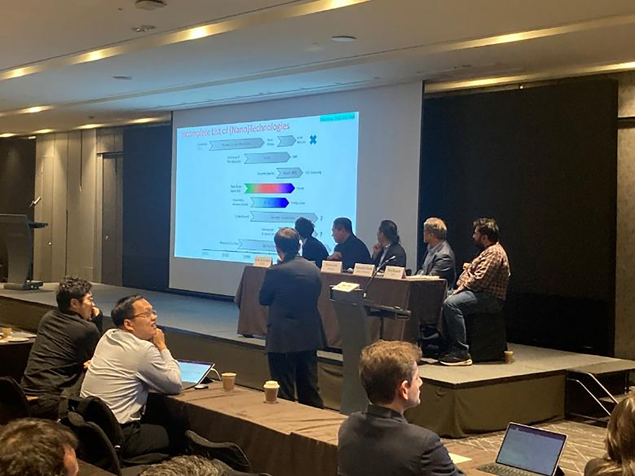
Panel Discussion on “Advanced channel materials for memory application”.
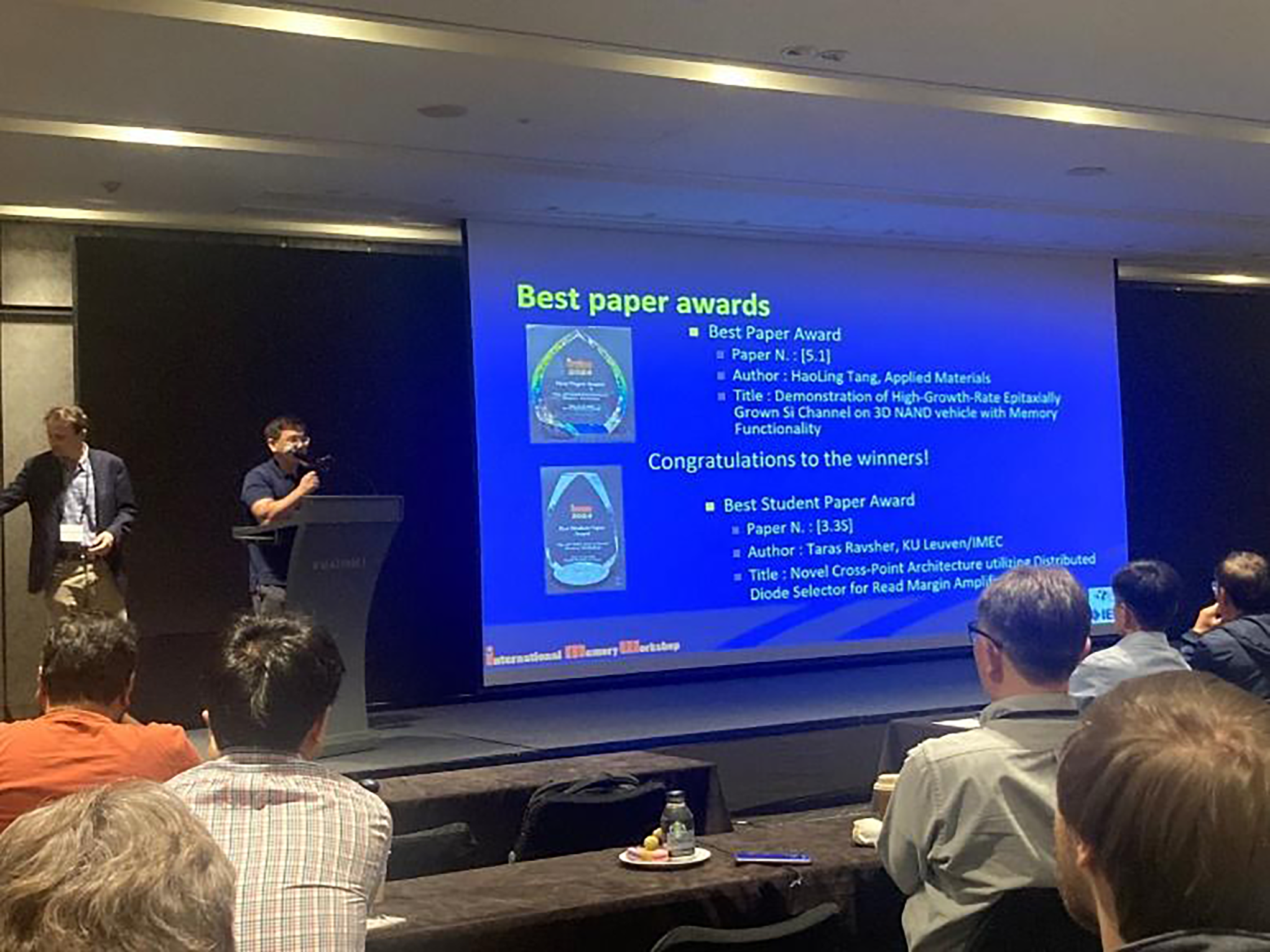
2024 Technical Chair Haitao Liu presenting the 2024 Best Paper and Best Student Paper Award winners.
The IMW is also an excellent forum to present new and original technical works and this year’s technical program comprised 33 excellent papers, which included 18 oral presentations and 15 posters. The papers were selected by the technical committee among more than 72 papers submitted and covered the major categories of memory technologies (3D NAND, 3D DRAM, Ferroelectric, STT, RRAM, PCM, and selectors) and NVM applications (Automotive, In-memory and Neuromorphic Computing).
Among the exciting news presented at the conference, the paper titled “Demonstration of High-Growth-Rate Epitaxially Grown Si Channel on 3D NAND vehicle with Memory Functionality” by Hao-Ling Tang (Applied Materials) won the Best Paper Award, and the paper, “Novel Cross-Point Architecture utilizing Distributed Diode Selector for Read Margin Amplification” presented by Taras Ravsher (KU Leuven/IMEC) received the Best Student Paper Award.
Different activities were organized to promote social contacts between the participants. The conference included lunch meals, a welcome reception (with a presentation of the posters), and a conference dinner. This year there were also some side activities that were not part of the official IMW program but made a very good addition. On the one side, students from Seoul National University (SNU) had the possibility to present their work in a poster exhibition and some two of the sponsors were present with a booth.
Another highlight of the conference was the panel discussion on the topic “Advanced channel materials for memory application” hosted by Jian Chen (Stanford University).
The next IMW will be held in May 2025 in Monterey, California, USA. For more details on the IMW conference please visit the IMW website: http://www.ewh.ieee.org/soc/eds/imw/. IMW technical proceedings are available on the IEEE Xplore database: https://ieeexplore.ieee.org/xpl/conhome/1002800/all-proceedings.
Thomas Mikolajick
2024 IMW Publicity Chair
 |
IEEE Collabratec Users Forum |  |
This community forum provides IEEE Collabratec users the opportunity to ask questions about the platform, report system problems, especially critical ones, and learn about new features and functionality on the platform. Users should avoid posting complex laundry lists, personal discussions, or other items that don’t relate to user issues. Also, unless you are CT Staff or have gone through Ambassador training, do not provide alternate training that may confuse users. Thank you!
Communities in IEEE Collabratec® offer a forum to: