2024 IEEE Symposium on VLSI
Technology & Circuits*

The 2024 IEEE Symposium on VLSI Technology & Circuits (VLSI Symposium) resumed in Honolulu, Hawaii, USA, attracting an all-time Symposium record Honolulu attendance of 1365 and 88% onsite participation! The Symposium was launched in 1981 with the initial vision of fostering open technical exchanges between Japanese and American researchers as well as bridging the divide between technologists and circuit designers. Now in its 44th consecutive year of alternating venues between Kyoto, Japan and Honolulu, Hawaii, USA, the Symposium continues to build on its established reputation as the microelectronics industry’s premiere international conference uniquely offering even more convergence in technology, circuits, and systems innovations unlike any other conference.
The Symposium took place from Sunday, 16 June to Thursday, 20 June 2024 at the Hilton Hawaiian Village Hotel. Unified by the theme of “Bridging the Digital and Physical Worlds with Efficiency and Intelligence”, the Symposium featured advanced technology developments, innovative circuit design, and the applications that they enable, as part of our global society’s transition to a new era of intelligent connected devices, energy-efficient infrastructure, and AI-enabled hardware systems that change the way humans interact with each other. The Symposium’s main offering comprised two Plenary sessions, 19 Technology sessions, 29 Circuits sessions, and six Joint Technology/Circuits sessions, drawing from a historical record of paper submissions. Furthermore, the program featured a demonstration session, an evening panel discussion, short courses, and workshops. Virtual access to the technical content became available the week following the onsite event until the end of August 2024.
Plenary Sessions
The Symposium launched the spirit of global collaboration between technology and circuit innovators with four plenary talks relevant to both camps. In his talk titled “Making Sense at the Edge”, Ahmad Bahai from Texas Instruments summarized advances in nanotechnology, analog and digital signal processing, embedded/edge machine learning algorithms, connectivity, and battery technology that have enabled unprecedented sensing and actuation performance, and turned to biological systems to inspire a future of significantly more efficient edge-computing sensory solutions. In his talk “Mobility Evolution: Electrification & Automation”, Kazuoki Matsugatani from DENSO examined key challenges in the automotive industry, namely environmental impact reduction and safety enhancement, to motivate the role of electrification and automation as solutions to these challenges. Maryam Rofougaran from Movandi offered her vision of wireless networks becoming the backbone of a hyperconnected world by providing high-speed, low-latency data transmission in “Wireless and the Future Hyperconnected World”. Finally, Hidehiro Tsukano from NTT shared an initiative in his talk titled “Photonics-Electronics Convergence Devices Accelerate IOWN (Innovative Optical Wireless Network)” to create a new optical-based information and communications technology platform that features high-capacity, high-quality, low-latency, and low-power consumption.

Plenary speakers Ahmad Bahai, Kazuoki Matsugatani, Maryam Rofougaran, and Hidehiro Tsukano.
Workshops and Short Courses
Sunday afternoon was reserved for four workshop sessions to warm up the Symposium attendees. The Technology workshop focused on novel metals and advanced interconnects, a critical area where innovations are essential to extend advanced CMOS scaling. The Circuits workshops showcased recent developments balancing analog and digital in high-performance mixed-signal PLL, ADC, and DAC circuits as well as covering biosensory breakthroughs for the future of health technology. There was also a standing workshop on open-source design, building on the inertia towards global democratization of chip design.

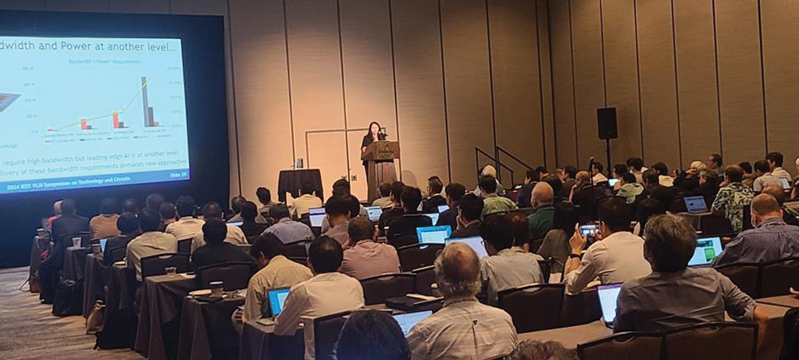
A scene from the short courses attended by over 700.
The Symposium Short Course featured two parallel full-day tracks on Monday. A perennial crowd favorite, the Technology Short Course spanned “Advanced VLSI Technologies for Next Generation Computing”, covering transistor scaling, interconnects, memory technology evolution, backside power delivery, process technologies, metrology and inspection, in-memory computing, and silicon photonics. The Circuits Short Course focused on “Circuits and Systems for Heterogeneous Integration” with industry experts addressing the latest advances in advanced packaging, die-to-die connectivity, memory co-integration, wafer-scale integration, heterogeneous integration for automotive application, integrated power delivery and management, and EDA tools for heterogeneous systems.
Demo Session
The demonstration session was held on Monday evening, providing participants an opportunity for lively in-depth engagement with authors of 16 selected papers from both Technology and Circuits sessions. Decided by participant voting, this year’s Best Demo Paper Awards were presented to K. Morimoto et al. from Canon for “3D-stacked 1-megapixel time-gated SPAD image sensor with 2D interactive gating network for image alignment-free sensor fusion” and to M. Liu et al. of the Chinese Academy of Sciences and University of Chinese Academy of Sciences for “First demonstration of monolithic three-dimensional integration of ultra-high density hybrid IGZO/Si SRAM and IGZO 2T0C DRAM achieving record-low latency (<10 ns), record-low energy (<10 fJ) of data transfer and ultra-long data retention (>5000 s).”

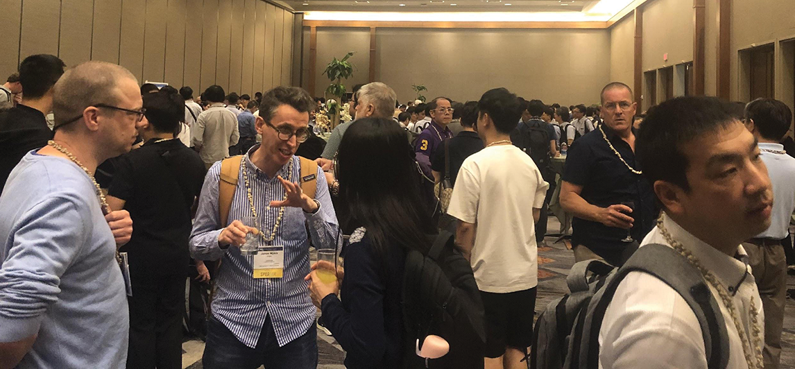
Attendees engaged in lively discussions with authors presenting demonstrations of their innovative work.
Technology Highlights
The Symposium showcased a plethora of technology innovations in advanced CMOS, memory, 3D, and beyond CMOS technologies.
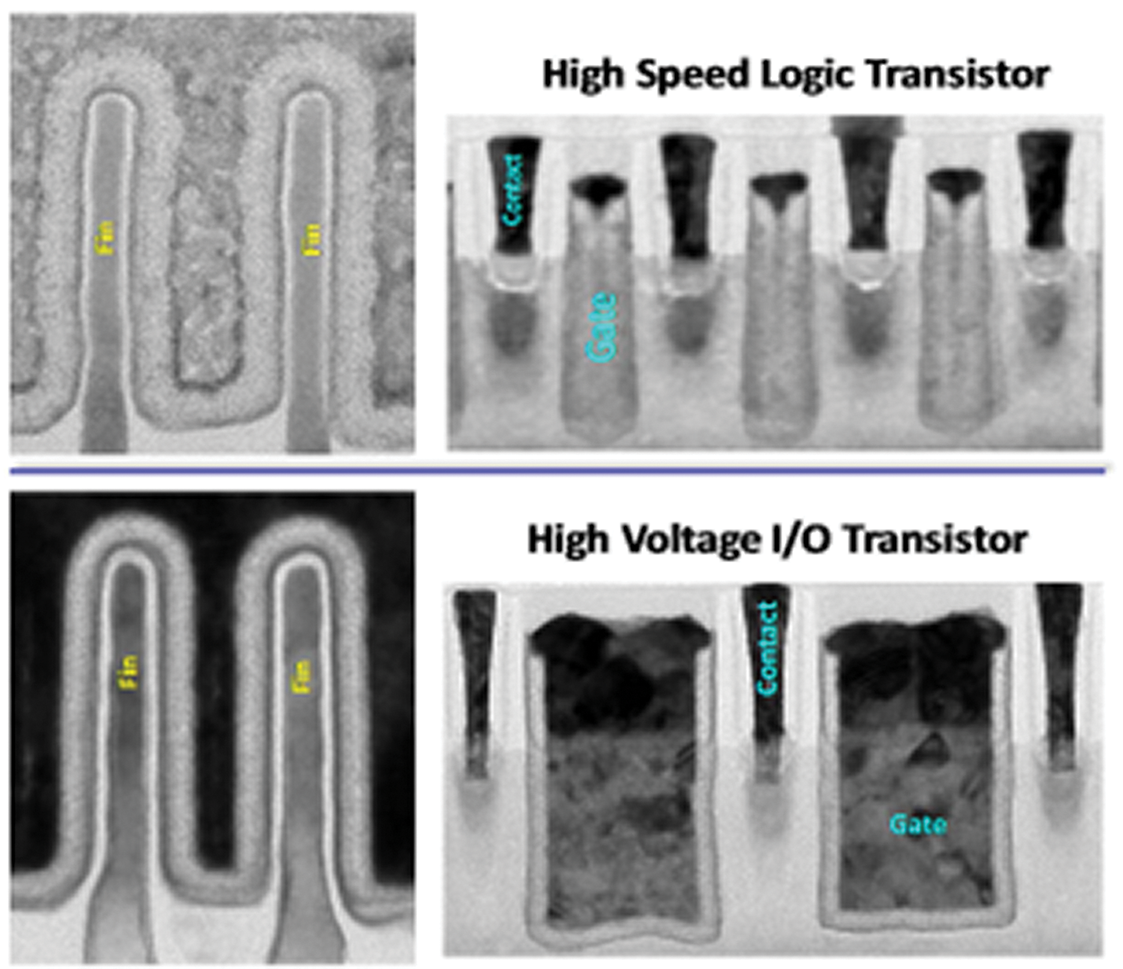
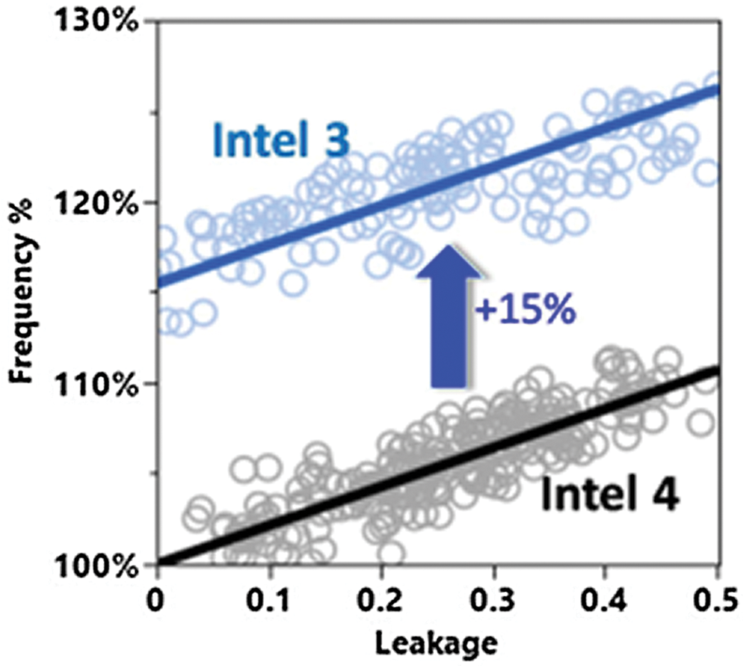
In the area of advanced CMOS, Intel presented its Intel 3 FinFET platform technology which offers 10% logic scaling, performance and reliability improvement compared to Intel 4 through transistor enhancements, interconnect optimization, and design co-optimizations. Intel 3 additionally enabled a 210 nm high-density standard cell, 1.2V-native I/O transistors, deep N-well isolation, and long-channel analog devices.
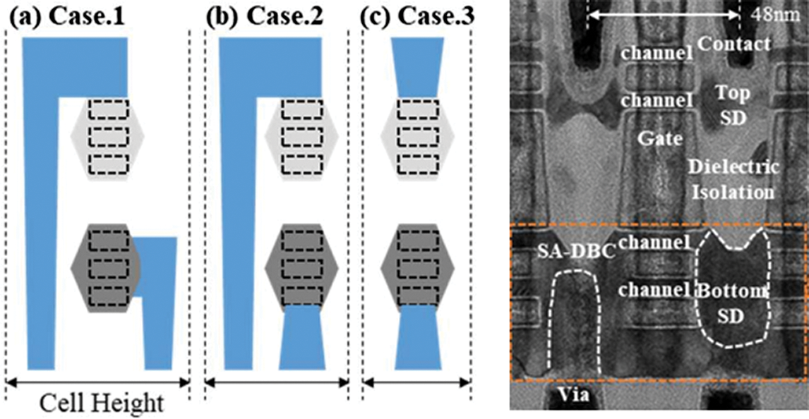
Beyond FinFET, Samsung demonstrated a 3D Stacked FET (3DSFET)—also known as Complementary FETs (CFETs)—with Self-Aligned Direct Back-side Contact (SA-DBC) and Back-side Gate Contact in 48-nm gate pitch, the smallest dimension reported to date. Simultaneous threshold voltage targeting for both nFET and pFET in a common gate and N/P connection with a common vertical contact were also verified to confirm the feasibility of scaling logic cell height beyond the 1-nm node.

Fin/gate TEM cross-section of logic and 1.2V I/O transistors (top/bottom respectively).

15% iso-leakage frequency enhancement in Intel 3 compared to Intel 4.

(Left) Various combinations of front-side contact and SA-DBC on 3DSFET reported by Samsung. (Right) Cross-sectional TEM image of co-integrated TOP-nFET and BOTTOM-pFET.
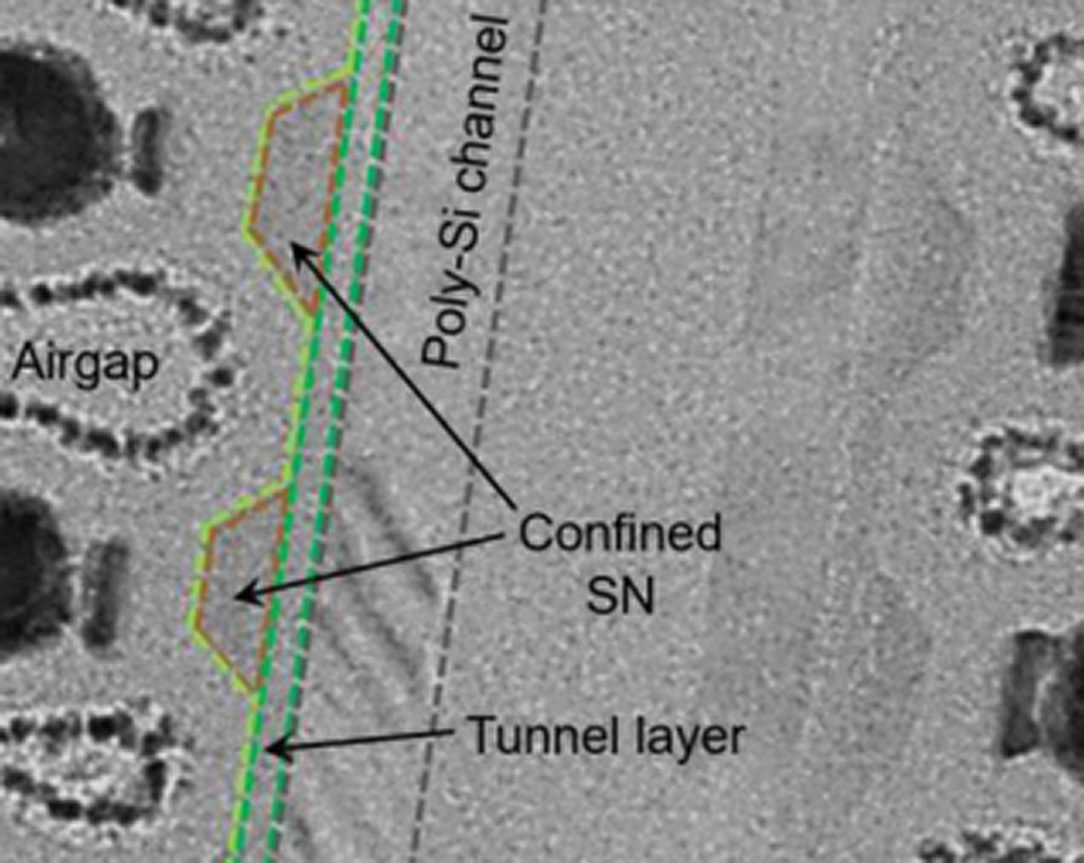
In the area of memories, Micron demonstrated a confined Storage Nitride 3D-NAND cell with an innovative process flow that enables a Word Line (WL) airgap to significantly reduce WL parasitic capacitance and faster programming time. Micron also reported on a stackable 4F2 polysilicon Thin Film Transistor (TFT) for ultra-dense 32-Gb NV (non-volatile) DRAM. Several key innovations such as pulsed laser annealing were implemented to meet the strict thermal budget constraints required for this dual-layer technology.
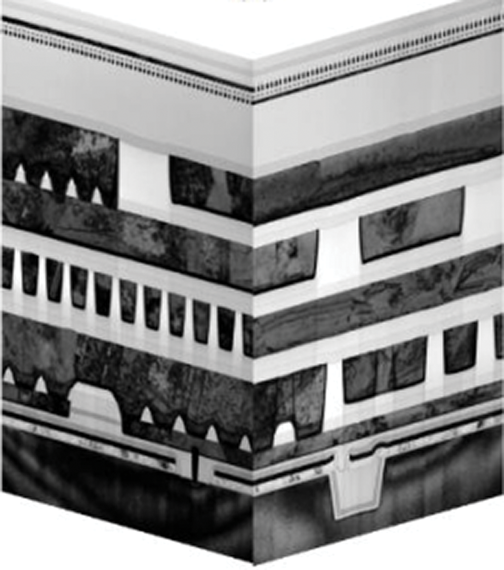
SK Hynix demonstrated the first fully integrated 16-nm half-pitch Selector Only Memory (SOM) for for emerging Compute Express Link™ (CXL) memory. SK Hynix achieved 750-mV read window margin including product-level raw bit error rate and reliability figures such as drift-related persistency, read disturbance, high temperature data retention (>10 years at 125 °C), and cycle endurance for 200 ppm raw bit error rate.

TEM cross-section of a single pillar in confined-Storage-Nitride cell 3D-NAND array with airgaps.

Cross-sectional image of dual-gated (Ru) TFT access device for NVDRAM.
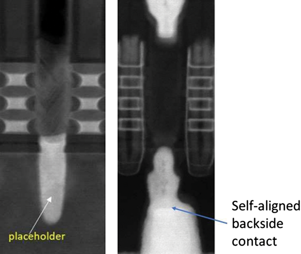
In the area of 3D integration, IBM and Samsung examined various approaches for integrating the backside power distribution (BSPDN) with stacked nanosheets for enabling beyond 2nm CMOS. Direct backside contact-based schemes offer the best logic cell scaling.
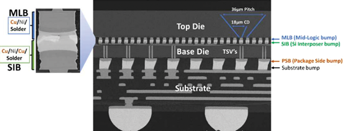
Intel presented the integration of High-Density Metal-Insulator-Metal (MIM) decoupling capacitors in a passive silicon interposer for supply voltage drop reduction and noise suppression. This technology offers interconnections among different chiplets using Through Silicon Via (TSV) technology along with a refined 36-μm microbump pitch in a face-to-face die configuration.

Cross-sectional TEM image of 16-nm half-pitch cross-point SOM with periphery under cell architecture.

TEM image of a transistor after placeholder and source/drain epitaxy formation and with self-aligned backside contact.
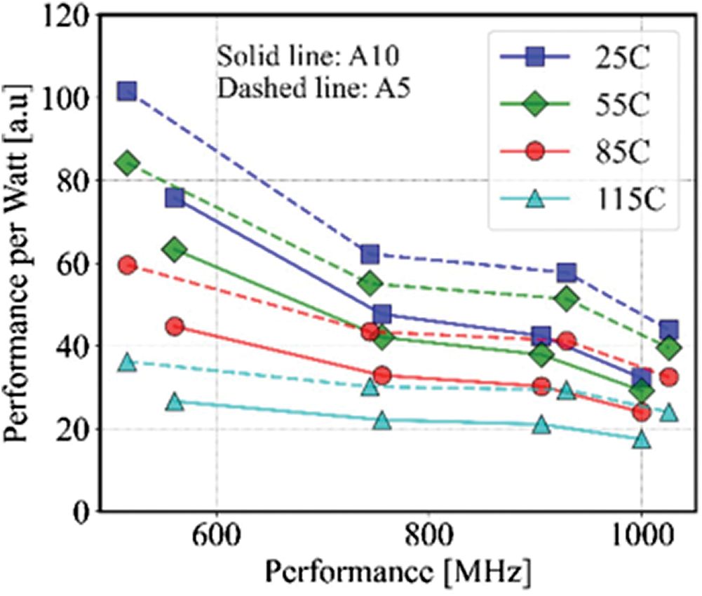
With CFETs likely to increase power density, IMEC conducted a timely and relevant analysis of thermally aware Power, Performance, and Area (PPA) in nanosheets and CFETs in future Ångstrom nodes termed A10 and A5 respectively. They reported block-level scaling results from A10 to A5 node on an open-source multi-core architecture: 2.5% increase in Fmax, 25% reduction in power, 27% reduction in energy per cycle, achieved with 35% area reduction and a consequent increase in power density by 15% under nominal condition of 0.7 V and 25 °C. The PPA analysis methodology was augmented with a fast package-level thermal simulator to enable early thermal estimation of system throughput.

Cross section showing interposer connection to top die through silicon interposer bump and package.

Performance/Watt comparison between A10 and A5 nodes, showing higher efficiency for A5 node across all temperatures.
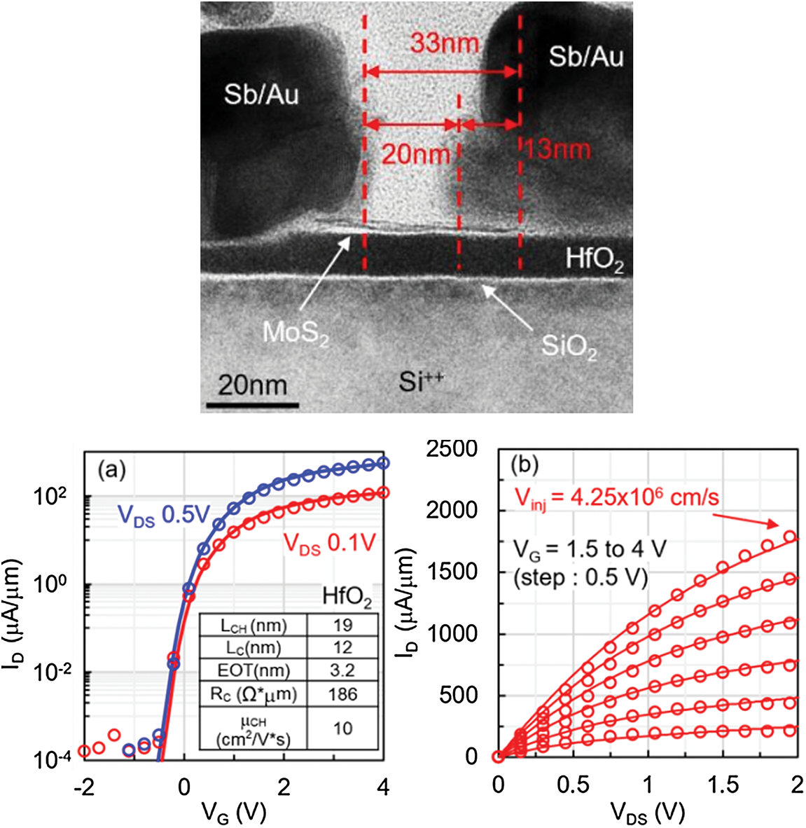
The latest exciting progress for beyond silicon-based devices continues to be reported at the Symposium. Collaborators at TSMC and National Yang Ming Chiao Tung University presented their recent results to scale transistors using 2D Transition Metal Dichalcogenide (TMD) materials such as MoS2. They demonstrated contact length scaling while holding a low contact resistance down to 11 nm. Channel length scaling shows ION can increase down to at least 12 nm with low RC. The very scaled (channel length = 19 nm) MoS2 transistor with Sb-based metal contact achieved a current density of ∼1130 μA/μm at VDS = 1 V, and a low contact resistance of ∼190 Ω·μm.

(Top) TEM images of MoS2 device showing aggressive scaling – channel length of 13 nm. (Bottom) Transfer and output characteristics of a device with 3.2 nm EOT. Symbols are experimental data, lines are TCAD model.

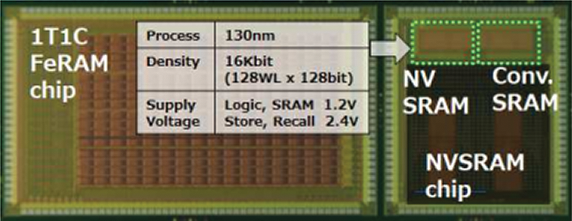
Photo image of Non-Volatile SRAM and Ferroelectric RAM chips formed on one wafer. The NVSRAM chip also has a conventional SRAM macro for comparison.

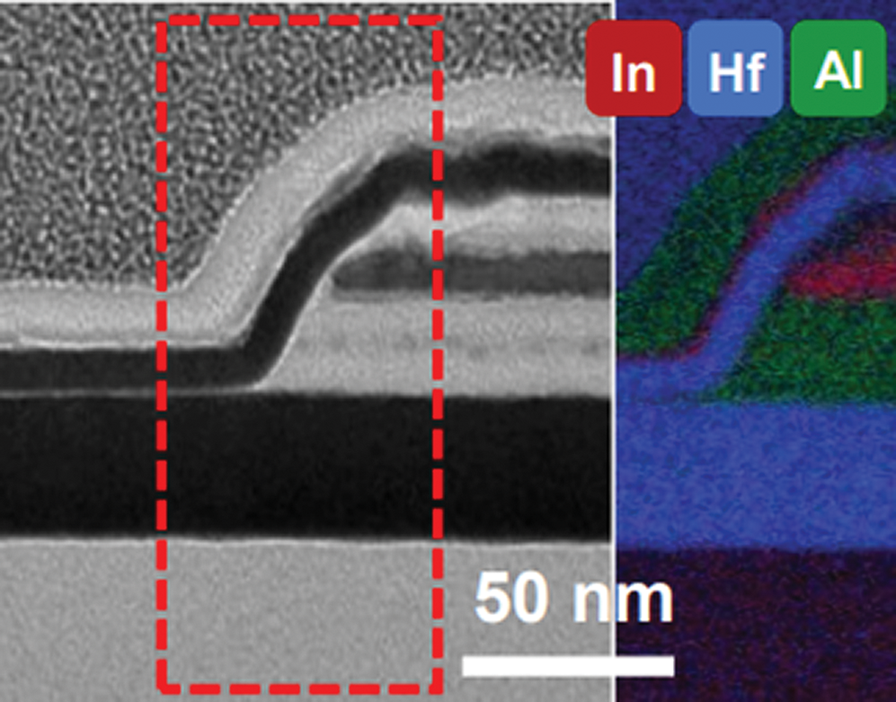
High-Resolution TEM cross-section image and EDS mapping of an ALD vertical all-oxide FET 10nm In2O3 dielectric.
In the area of metal oxide devices, Sony and its collaborators at Fraunhofer IPMS and NaMLab experimentally demonstrated 100%-bit yield on a 16 kbit Non-Volatile SRAM (NV-SRAM) array based on a metal/ferroelectric/metal capacitor using a sub-10 nm thick HfZrOx (HZO) layer. These results indicate that HZO-based NV-SRAM and FeRAM hybrid memory system can provide ultra-low power advantages in a System-on-Chip for Internet-of-Things edge computing.
In the area of all-oxide transistors, collaborators at Purdue University and Samsung reported for the first time atomic-layer-deposited (ALD) all-oxide transistors toward 3D vertical integration, with thick ALD In2O3 as gate electrodes and In2O3 itself as the contact. The all-oxide TFTs show an on/off ratio over 106, high uniformity, and robust bias-temperature stress reliability.
Circuits Highlights
The Symposium continues to be the premier venue where researchers report the latest in circuits demonstrations pushing the envelope of PPA and integration levels in many fronts.
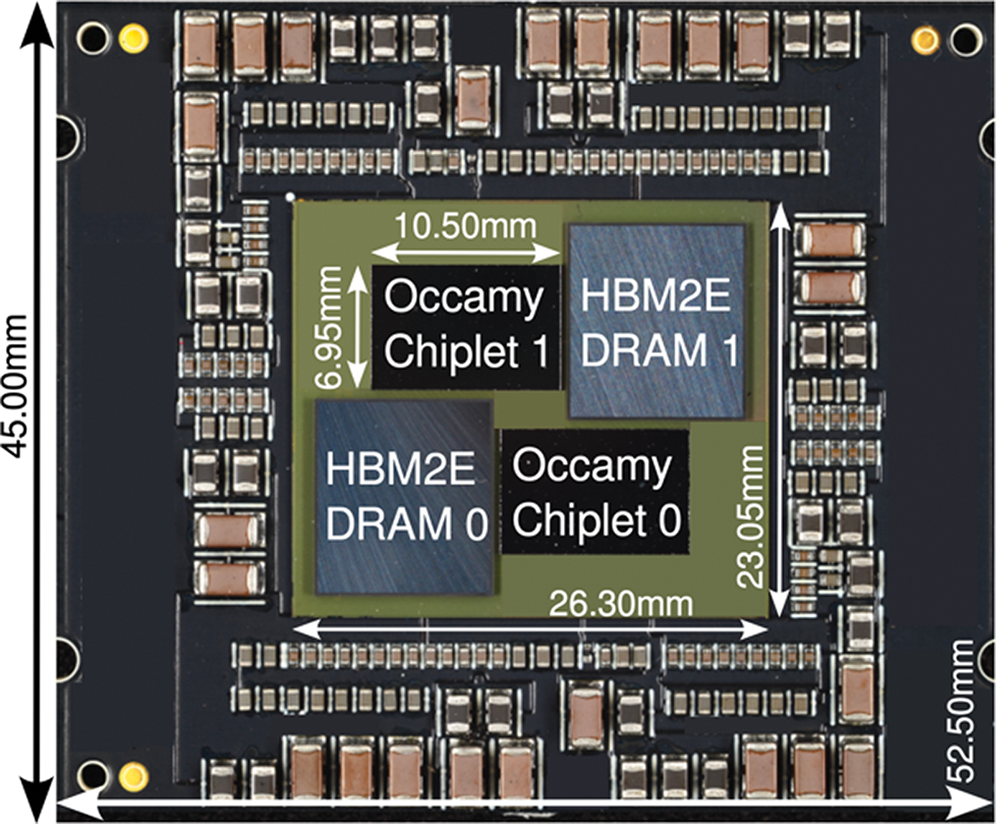
In the processor and SoC domain, collaborators at ETH Zürich, Stanford University, and the University of Bologna presented a flexible, general-purpose, dual-chiplet system with two 16 GB HBM2E stacks optimized to address a wide range of irregular-memory-access compute workloads with high utilization. Codenamed Occamy, the heterogeneous system comprises a 432-core RISC-V dual-chiplet 2.5-D system for efficient sparse linear algebra and stencil computations on FP64 and narrow (32-, 16-, 8-bit) SIMD floating-point data. Occamy features 48 clusters of RISC-V cores with custom extensions, two 64-bit host cores, and a latency-tolerant multi-chiplet interconnect and memory system with 32 GB of HBM2E. Silicon demonstrates leading-edge utilization on stencils (83%), sparse-dense (42%), and sparse-sparse (49%) matrix multiplication.

Dual-chiplet module photograph.
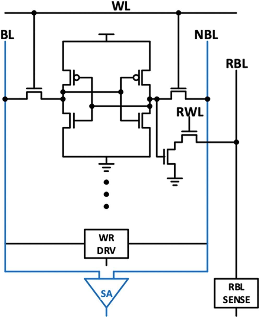
In the area of memory circuits, authors from Arm demonstrated a 1Read-1ReadWrite (1R1RW) High Bandwidth Instance (HBI) L1-data cache memory architecture in 3 nm CMOS which is seamlessly integrated into Arm’s flagship high-performance processor. Enhancing the conventional 8T-1R1W memory, HBI features an additional read port to achieve 1R1RW capability, doubling the available read bandwidth and enabling 13% area reduction and 10–15 ps routing delay reduction. Silicon demonstrates 1R1RW HBI yield of 100% yield, the highest reported frequency of over 7 GHz and lowest reported bit density of 11.2 Mbit/mm2 for any 8T SRAM memory.

1R1RW HBI memory cell architecture offering 33% reduction in L1-Data cache area compared to 6T-1RW memory.
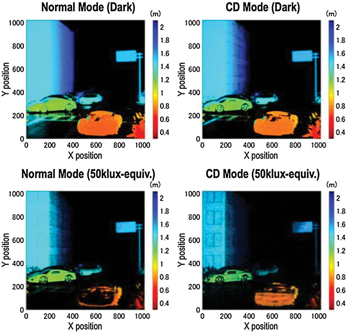
Related to imager circuits, Canon presented a 5μm-pitch, 3D-BSI 1Mpixel time-gated SPAD image sensor featuring 2D interactive gating network, enabling image alignment-free sensor fusion. The device operates at 1,310 fps for global shutter 2D imaging, and event vision sensing with 0.76-ms temporal resolution under 0.02 lux. Through range-gated imaging, this work demonstrated a feasibility of robust imaging under harsh environments. The gating network architecture enables background suppression in 3D depth measurement under 50 klux ambient light.
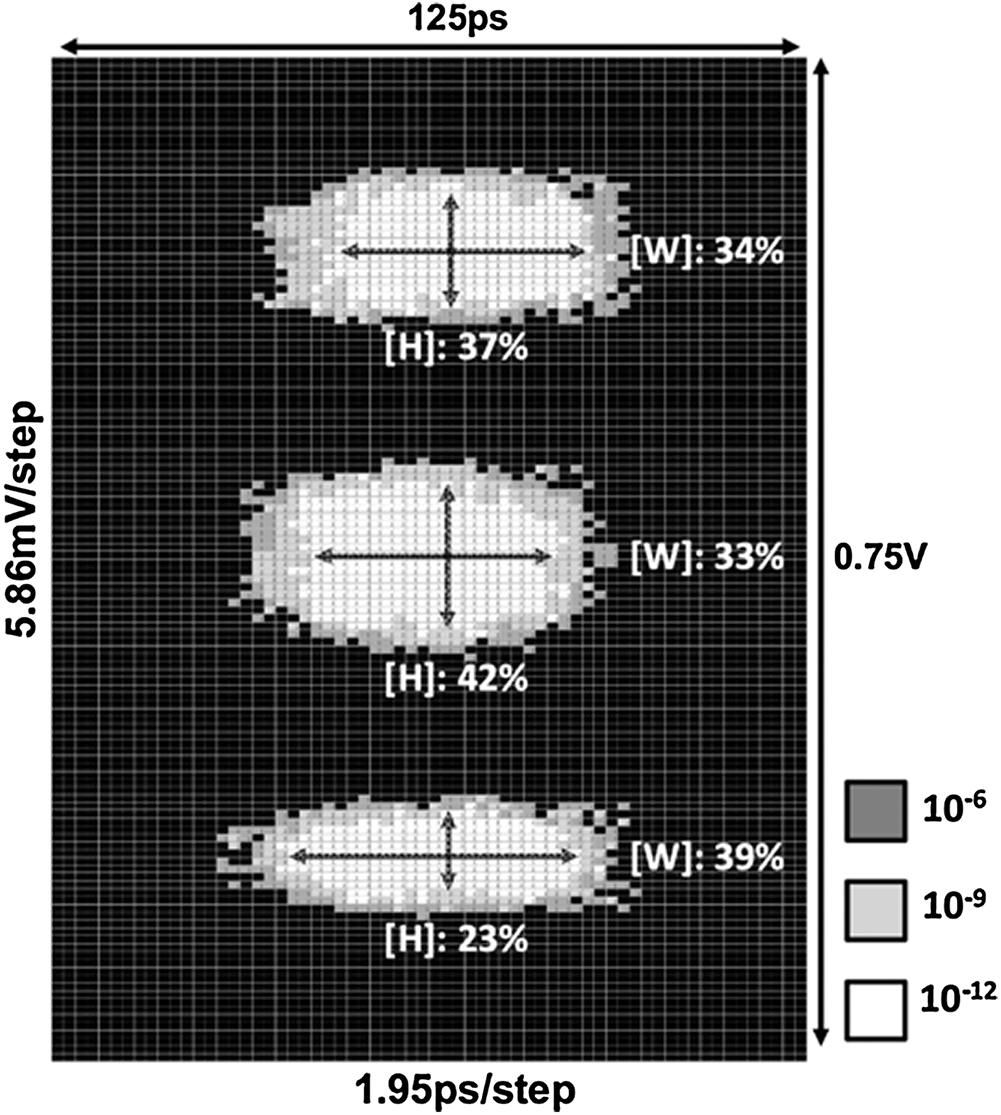
Migration towards heterogeneous systems has motivated intense development of within-package links. Authors at TSMC presented a die-to-die link for heterogeneous integration of a 5-nm compute die and 6-nm SRAM die with face-to-back 3D stacking at a 9-μm bond pitch. The work demonstrated modular design that supports full scalability and achieves 10.24-Tb/s aggregate bandwidth for 320 TX lanes and 320 RX lanes, at a PAM-4 16 Gb/s per lane data rate. Each data cluster module comprises 80 TX/RX lanes in a 378 μm × 378 μm footprint to offer a bandwidth density of 17.9 Tb/s/mm2 and an energy efficiency of 0.296 pJ/bit per link.

Measured 3D depth maps with normal- and CD-mode, captured under dark and 50klux-equivalent ambient light.

Measured PAM-4 eye at 16 Gb/s.
A lot of other circuit- and system-related topics were covered during VLSI 2024. To name a few only, circuits for machine learning, security, biomedicine, data conversion, analog/mixed-signal, optical link, and RF domains were broadly represented in numerous sessions. Their presentation is beyond the scope of this wrap-up. They will be presented in IEEE Solid-State Circuits Magazine.
Evening Panel
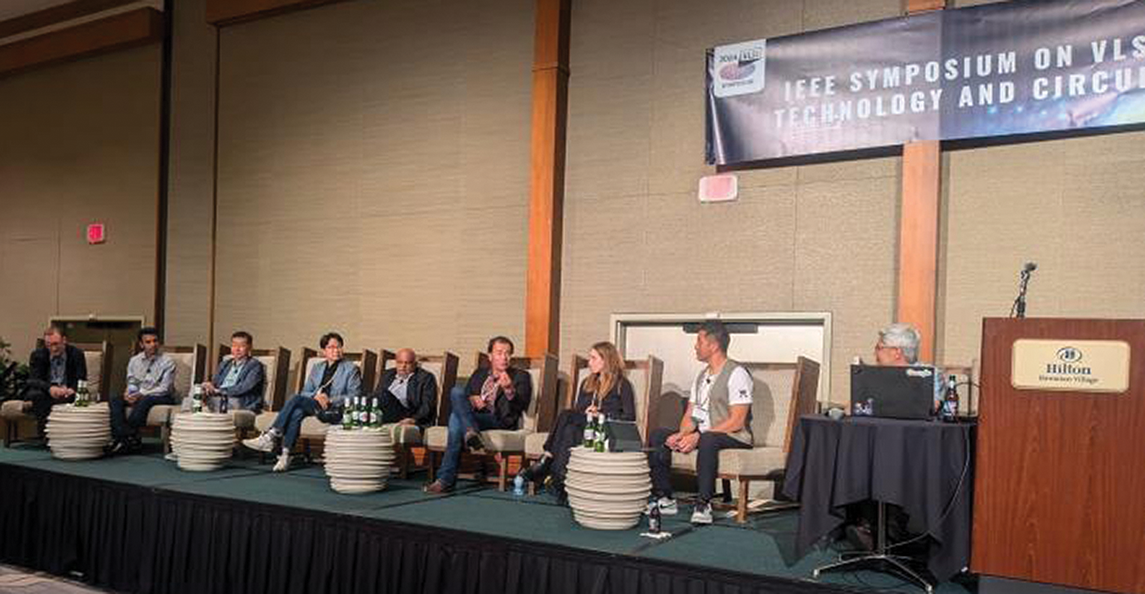
The joint Technology/Circuits evening panel took place on Tuesday evening to debate the question “Will AI bite the industry that feeds it?” After panelists shared their perspectives on whether AI will take over humanity, Patrick Yue from HKUST and Stacy Ho from Mediatek hosted a fun and engaging exchange with the audience who asked tough AI-related questions such as “is it too late to buy Nvidia stock?”. The panelists would then compete against Google Gemini to provide the best answers.

Panelists compete with Google Gemini to answer audience questions.
Special Events
The luncheon talk resumed for the first time since the COVID pandemic. On Thursday, Greg Yeric from the U.S. Department of Commerce spoke on “The CHIPS Program and You: An R&D Update for the VLSI Symposia”.
The Symposium continues to offer a well-attended mentoring event hosted by IEEE Women in Engineering and Young Professionals, sponsored by the IEEE Electron Devices Society and Solid-State Circuits Society.
Symposium Awards
The Test of Time Award, established in 2021, was presented for the fourth time in the Symposium history to recognize seminal Symposium contributions published at least a decade ago that have earned historical significance. This year’s very deserving recipients were C. P. Yue and S. S. Wong from Stanford University for their paper “On-chip spiral inductors with patterned ground shields for Si-based RF IC’s” from 1997 and L. Chang et al. from IBM for their paper “Stable SRAM cell design for the 32 nm node and beyond” from 2005.
Also announced at this year’s Symposium was the Best Student Paper Award for last year’s Symposium, a tradition dating back to 2004. The recipients were “Foundry monolithic 3D BEOL transistor + memory stack: iso-performance and iso-footprint BEOL carbon nanotube FET+RRAM vs. FEOL silicon FET+RRAM” by A. C. Yu from Massachusetts Institute of Technology and “An energy-efficient impedance-boosted discrete-time amplifier achieving 0.34 noise efficiency factor and 389 MΩ input impedance” by G. Atzeni et al. from ETH Zurich.
Celebration of Contributions and Friendships
The social highlight of the Symposium was none other than the traditional Hawaiian luau banquet on Wednesday evening. There were plenty of reasons to celebrate – incredible progress in our industry, all-time high paper submissions and record Honolulu attendance after 44 years, a third year offering a hybrid format, plenty of high-quality online content, and of course, the in-person experience in Hawaii to reconnect with old friends and meet new ones. Heartfelt thanks to the many SSCS/EDS organizers, Symposium Secretariat, and the committee member family who all worked tirelessly to make the Symposium a true success! A special shout out goes to Phyllis Mahoney who has retired from the Symposium after decades of service managing the Symposium.

Participants enjoying entertainment at the Wednesday luau.
The VLSI Symposium returns to Kyoto, Japan— ranked 5th best place in the world to visit by National Geographic – on 12–16 June 2025. Visit vlsisymposium.org for the latest updates. Paper submissions are due on 27 January 2025. A hui hou i keia makahiki ae! (See you again next year!)
Alvin Loke, Publicity Chair
Franck Arnaud, Publication Chair
Masahiko Kanda and Takashi Tokuda, Publicity Co-Chairs
* An extended version of the article will be included in the upcoming issue of IEEE Solid-State Circuits Magazine

Engineer your future with the IEEE Learning Network (ILN).
Explore hundreds of continuing education courses from IEEE, all in one place.
Featured Topics:
- Computing
- Emerging Technologies
- English for Technical Professionals
- Power and Energy
- Telecommunications
- IEEE Standards
Access: https://iln.ieee.org/public/TrainingCatalog.aspx

